Low depth combinational finite field multiplier

a combinational finite field and low depth technology, applied in the field of multiplier circuit designs, can solve the problem of almost infeasible security support of software data, and achieve the effect of easy testing and debugging

Inactive Publication Date: 2016-08-16
INTEL CORP
View PDF17 Cites 1 Cited by
  • Summary
  • Abstract
  • Description
  • Claims
  • Application Information

AI Technical Summary

Benefits of technology

[0011]The objects, features and advantages of the present invention include providing a method and / or apparatus for implementing a low depth combinational finite field multiplier that may (i) be used in high throughput implementations, (ii) implement an area efficient circuit, (iii) provide flexible and parameter-based multiplier construction, (iv) provide scalable unified netlist generation and / or (v) enable easy testing and debugging.

Problems solved by technology

The high speeds alone make security support of the data in software (SW) almost infeasible as far as security transformations are usually incorporated into the main data path and appear as bottlenecks from efficiency and performance standpoints.

Method used


Image

  • Low depth combinational finite field multiplier
  • Low depth combinational finite field multiplier
  • Low depth combinational finite field multiplier

Examples


Embodiment Construction

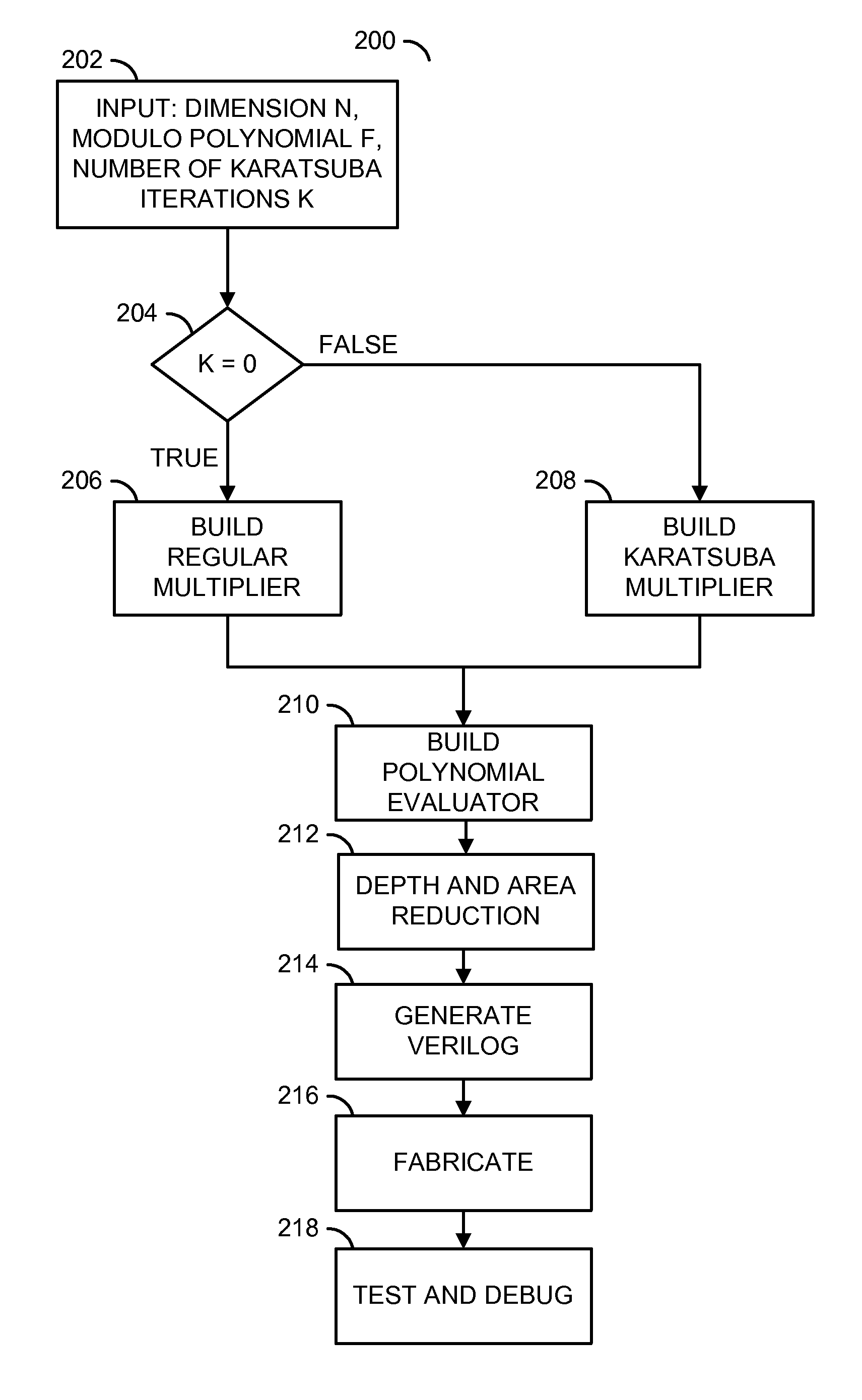
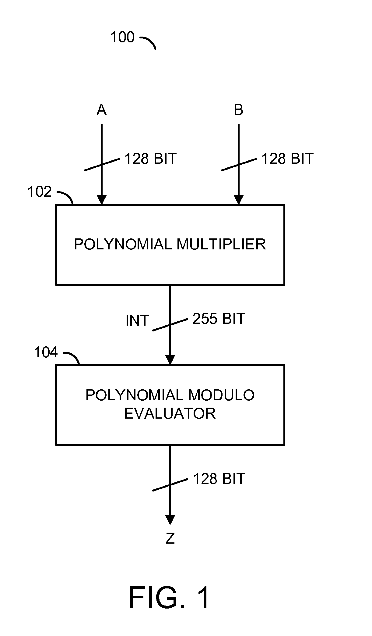
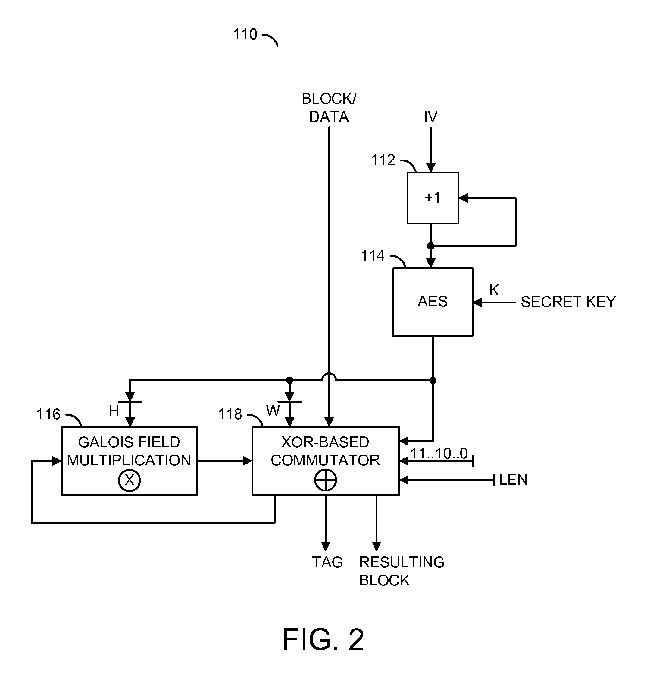
[0023]Some embodiments of the present invention generally describe an implementation method for a low gate-depth finite field multiplier for the high throughput cryptographic applications. The method of multiplier implementation may be based on the Karatsuba scheme. The implementation generally leads to low depth of the combinatorial circuit that allows use in the high throughput implementations of GCM-AES, LRW-AES, Universal mobile telecommunications system Integrity Algorithm 2 (UIA2) (e.g., Snow 3G) and other cryptographic applications by providing an instantiated 1-cycle multiplier in such applications. The multiplication scheme may support many applications in data security and storage plus Internet and wireless applications related to data protection. Error correcting codes dealing with Galois Field multiplication may also be applicable.

[0024]The resulting circuits are generally performance and area efficient with memory free combinatorial circuits of low depth and reduced are...


PUM


Abstract

A method for generating a design of a multiplier is disclosed. The method generally includes steps (A) to (C). Step (A) may generate a first circuit comprising a plurality of polynomial results of a particular multiplier scheme based on a plurality of parameters of the multiplier. The first circuit is generally configured to multiply a plurality of polynomials. Step (B) may generate a second circuit comprising a plurality of polynomial evaluators based on the parameters. The second circuit may be (i) connected to the first circuit and (ii) configured to evaluate a polynomial modulo operation. Step (C) may generate the design of the multiplier in combinational logic by optimizing a depth of a plurality of logic gates through the first circuit and the second circuit. A product of the polynomials generally resides in a finite field.

Description

[0001]This application claims the benefit of Russian Application No. 2011107568, filed Mar. 1, 2011 and is hereby incorporated by reference in its entirety.FIELD OF THE INVENTION[0002]The present invention relates to multiplier circuit designs generally and, more particularly, to a method and / or apparatus for implementing a low depth combinational finite field multiplier.BACKGROUND OF THE INVENTION[0003]Modern application-specific integrated circuits (ASICs) integrate greater and greater security and data protection functionality into the hardware (HW). The integrated functionality provides more reliable and more efficient hardware security for both conventional “Data At-Rest” and conventional “Data In-Flight” protection.[0004]Data storage systems are moving to distributed storage models that are based on storage networking. The move has an impact for enterprise data protection: the distributed models increase the vulnerability of stored data (i.e., Data At-Rest) to various attacks,...

Claims


Application Information

Patent Timeline
Patent Type & Authority Patents(United States)
IPC IPC(8): G06F7/72G06F17/50
CPCG06F7/724G06F17/505G06F30/327
Inventor GASHKOV, SERGEY B.BOLOTOV, ANATOLI A.GRINCHUK, MIKHAIL I.IVANOVIC, LAV D.CHASOVSHIKH, ANATOLY A.GALATENKO, ALEXEI V.KUCHERENKO, IGOR V.
Owner INTEL CORP
Why Eureka
Try Eureka