Bulk semiconducting scintillator device for radiation detection

a semi-conducting scintillator and radiation detection technology, applied in the direction of semiconductor devices, x/gamma/cosmic radiation measurement, instruments, etc., can solve the problems of poor phase homogeneity and achieve the effect of improving purity and homogeneity and poor phase homogeneity

Active Publication Date: 2016-08-30
CONSOLIDATED NUCLEAR SECURITY +1
View PDF3 Cites 1 Cited by
  • Summary
  • Abstract
  • Description
  • Claims
  • Application Information

AI Technical Summary

Benefits of technology

[0010]In various exemplary embodiments, the present disclosure provides a multistep synthetic process for synthesizing an inorganic compound with unique electrical and optical properties. This compound is semiconducting and can be developed for nonlinear optical applications, as well as radiation detection. The I-III-VI2 stoichiometry crystallizes into a chalcopyrite type structure, and when the Group I element is lithium, the material is potentially ideal for the room temperature detection of neutrons, for example. The best known synthesis method, described in U.S. Pat. No. 7,687,780 (Bell et al.), involves heating stoichiometric quantities of the three elemental powders simultaneously to form the I-III-VI2 compound. For the lithium containing compounds, lithium reactivity is difficult to control, leading to poor phase homogeneity. Thus, the present disclosure provides improved methods for combining the elemental constituents in a multistep synthetic process. These methods provide improved purity and homogeneity and more precisely control the reaction rate, thereby yielding a I-III-VI2 charge with a single phase stoichiometry.

Problems solved by technology

For the lithium containing compounds, lithium reactivity is difficult to control, leading to poor phase homogeneity.

Method used


Image

  • Bulk semiconducting scintillator device for radiation detection
  • Bulk semiconducting scintillator device for radiation detection
  • Bulk semiconducting scintillator device for radiation detection

Examples


exemplary embodiment 10

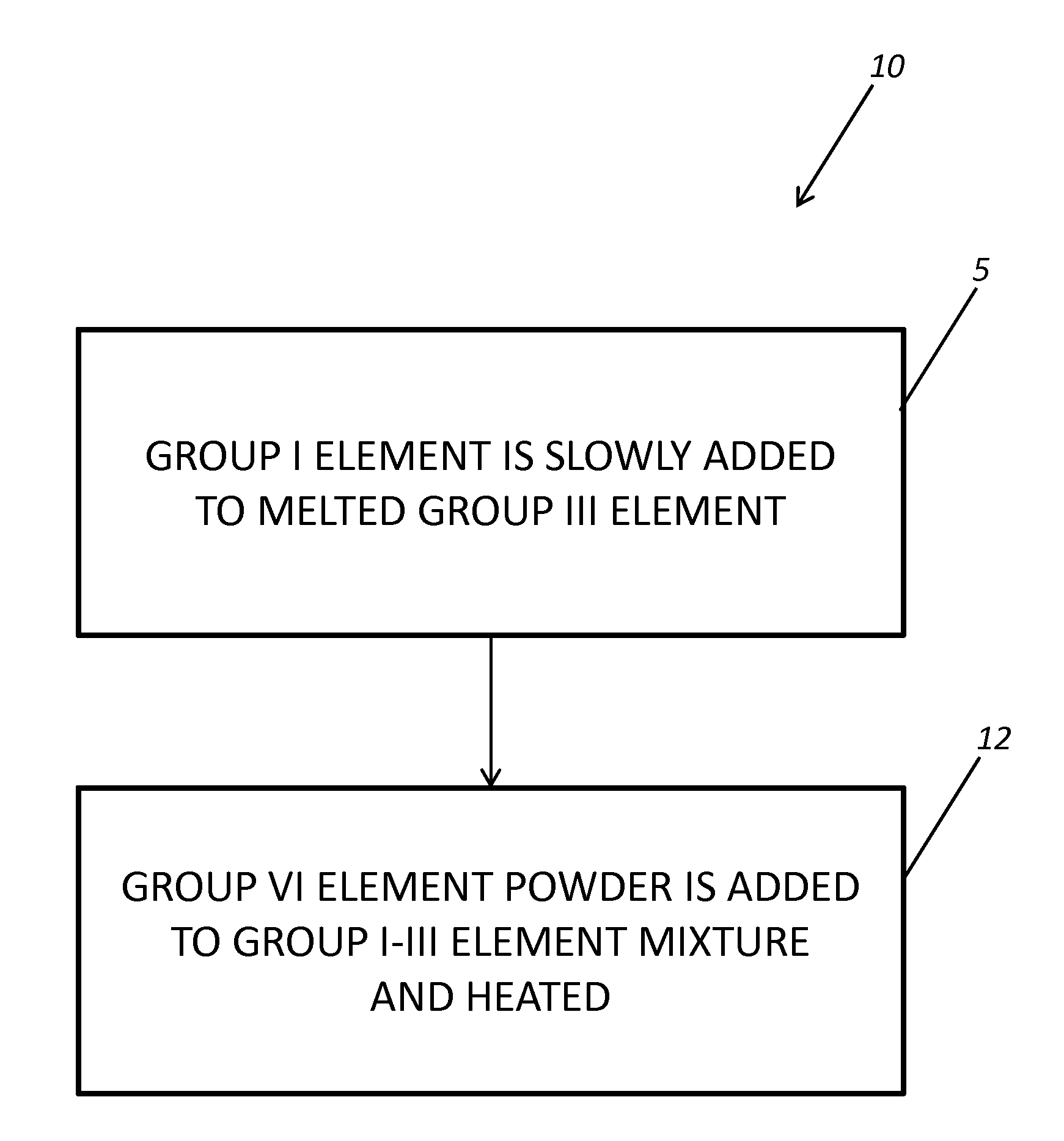
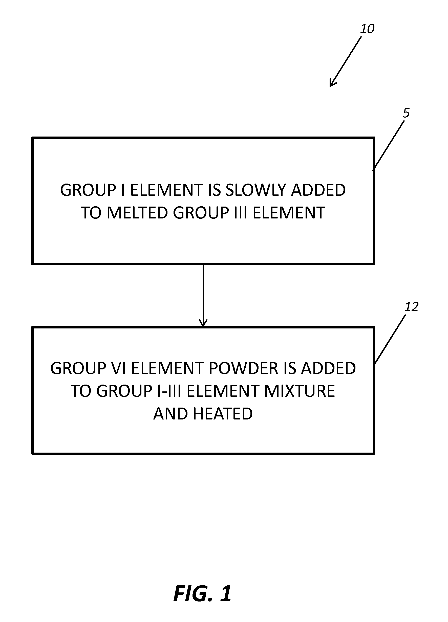
[0037]Referring specifically to FIG. 1, in the first exemplary embodiment 10, the Group VI elemental powder is added directly to the I-III alloy and heated to 700-900 degrees C. (depending on the group VI element) in a crucible (step 12). The reaction is allowed to proceed to completion and then cooled. Because the I-III compound is formed in an initial reaction step, the stoichiometry is defined as one mole for each element. Addition of the Group VI element for the final I-III-VI reaction has lower overall stoichiometric variability throughout the charge.

exemplary embodiment 20

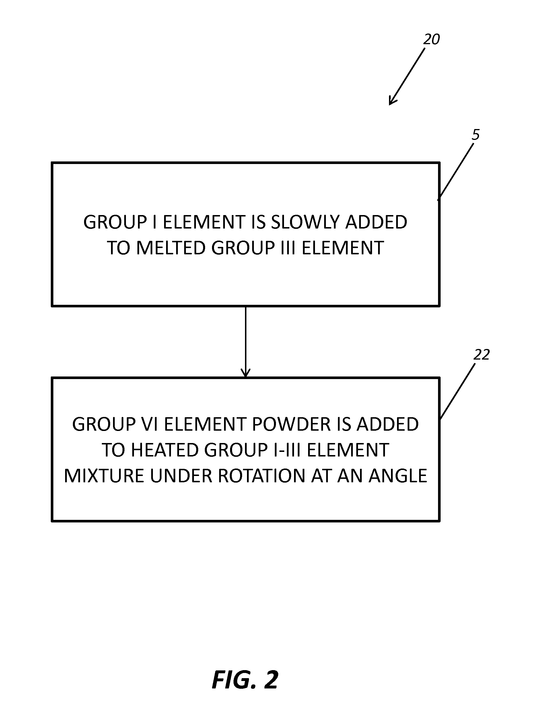
[0038]Referring specifically to FIG. 2, in the second exemplary embodiment 20, the addition of the Group VI element into a single crucible is as with the first exemplary embodiment; however, the constituents are mixed at elevated temperature with constant crucible rotation at an angle (step 22), for example about 20 degrees. Rotation further promotes mixing during the synthesis to reduce phase variability.

exemplary embodiment 30

[0039]Referring specifically to FIG. 3, the third exemplary embodiment 30 involves vapor transport of the Group VI element (step 32). The previously prepared I-III compound is placed in one well of a crucible, while the Group VI element is placed in an adjacent well. As the mixture is heated to 700-900 degrees C., the Group VI element slowly vaporizes and is transported through thermal currents to the melted group I-III well. The reaction then occurs to form I-III-VI2. Vapor transport further slows the reaction to minimize overheating and promote a single phase synthetic charge.

[0040]It should be noted that the methods of the present invention are not limited to the synthesis of semiconductor materials. Doping with an activator (e.g., Group IV element) may be performed to create a scintillator material, for example.

[0041]Referring now specifically to FIG. 4, the class of Li-containing semiconductor compounds of general composition Li-III-VI2, where III is a Group III element, such a...


PUM

PropertyMeasurementUnit
temperaturesaaaaaaaaaa
band gapsaaaaaaaaaa
band gapsaaaaaaaaaa

Abstract

A bulk semiconducting scintillator device, including: a Li-containing semiconductor compound of general composition Li-III-VI2, wherein III is a Group III element and VI is a Group VI element; wherein the Li-containing semiconductor compound is used in one or more of a first mode and a second mode, wherein: in the first mode, the Li-containing semiconductor compound is coupled to an electrical circuit under bias operable for measuring electron-hole pairs in the Li-containing semiconductor compound in the presence of neutrons and the Li-containing semiconductor compound is also coupled to current detection electronics operable for detecting a corresponding current in the Li-containing semiconductor compound; and, in the second mode, the Li-containing semiconductor compound is coupled to a photodetector operable for detecting photons generated in the Li-containing semiconductor compound in the presence of the neutrons.

Description

CROSS-REFERENCE TO RELATED APPLICATION[0001]The present patent application / patent is a continuation-in-part (CIP) of co-pending U.S. patent application Ser. No. 13 / 658,591, filed on Oct. 23, 2012, and entitled “METHODS FOR SYNTHESIZING SEMICONDUCTOR QUALITY CHALCOPYRITE CRYSTALS FOR NONLINEAR OPTICAL AND RADIATION DETECTION APPLICATIONS AND THE LIKE,” the contents of which are incorporated in full by reference herein.STATEMENT REGARDING FEDERALLY SPONSORED RESEARCH OR DEVELOPMENT[0002]The U.S. Government has rights to the present disclosure pursuant to Contract No. AC05-00OR22800 between the U.S. Department of Energy and Babcock and Wilcox Technical Services Y-12, LLC.FIELD OF THE DISCLOSURE[0003]The present disclosure relates generally to methods for synthesizing semiconductor quality chalcopyrite crystals for nonlinear optical and radiation detection applications and the like. More specifically, the present disclosure relates to methods for synthesizing a semiconductor detector of...

Claims


Application Information

Patent Timeline
Patent Type & Authority Patents(United States)
IPC IPC(8): G01T1/20G01T1/202G01T3/08C30B29/46
CPCG01T1/2023G01T3/08C30B29/46
Inventor STOWE, ASHLEY C.BURGER, ARNOLDGROZA, MICHAEL
Owner CONSOLIDATED NUCLEAR SECURITY
Why Eureka
Try Eureka