Semiconductor device

a technology of semiconductor elements and devices, applied in semiconductor devices, semiconductor/solid-state device details, electrical devices, etc., can solve the problems of increasing the temperature of the semiconductor element, the heat generated by the semiconductor element, and the deformation of the silicon gel, so as to prevent the occurrence of cracks, prevent the progress of thermal oxidation degradation, and improve the reliability of the semiconductor device

Active Publication Date: 2016-09-13
FUJI ELECTRIC CO LTD
View PDF25 Cites 2 Cited by
  • Summary
  • Abstract
  • Description
  • Claims
  • Application Information

AI Technical Summary

Benefits of technology

[0020]According to the semiconductor device of the invention, a nanocomposite resin is used as one of the sealing materials. Therefore, it is possible to protect, for example, a semiconductor element which is an internal structure of the semiconductor device. In particular, it is possible to suppress the progress of thermal oxidation degradation in a sealing portion of the semiconductor device for a long time, to prevent the occurrence of a crack, and to improve the reliability of the semiconductor device. As a result, the invention can be appropriately used in a semiconductor device using a wide-bandgap semiconductor element, such as a SiC or a GaN semiconductor element.

Problems solved by technology

However, when the current density of the semiconductor element increases, the amount of heat generated from the semiconductor element increases and the temperature of the semiconductor element increases.
When a general silicon gel according to the related art is used as the sealing material, in some cases, the silicon gel is degraded by oxidation at a high temperature of 175° C. or higher in an oxygen atmosphere and a crack occurs.
In addition, when a general epoxy resin is used as the sealing material, in some cases, the resin is similarly degraded by oxidation and a crack occurs.
However, in known techniques, it is difficult to maintain sealing characteristics at a high temperature of, for example, 175° C. or higher in the SiC or GaN semiconductor elements which operate at a high temperature.

Method used


Image

  • Semiconductor device
  • Semiconductor device
  • Semiconductor device

Examples


first embodiment

[0025]According a first embodiment of the invention, a semiconductor device includes: a molded body that is obtained by sealing, with a sealing material, a member including a semiconductor element, an insulating substrate which is bonded to one surface of the semiconductor element, and a printed circuit board which is used for a connection to an external circuit and is bonded to the other surface of the semiconductor element; and a sealing portion with a two-layer sealing structure in which a first sealing material that is a nanocomposite resin including an epoxy base resin, a curing agent, and an inorganic filler with an average particle size of 1 nm to 100 nm forms a first sealing layer that covers the semiconductor element and is provided in a region adjacent to the semiconductor element and a second sealing material that is a thermosetting resin, a thermoplastic resin, or a mixture thereof forms a second sealing layer that covers the first sealing layer and forms an outer surfac...

second embodiment

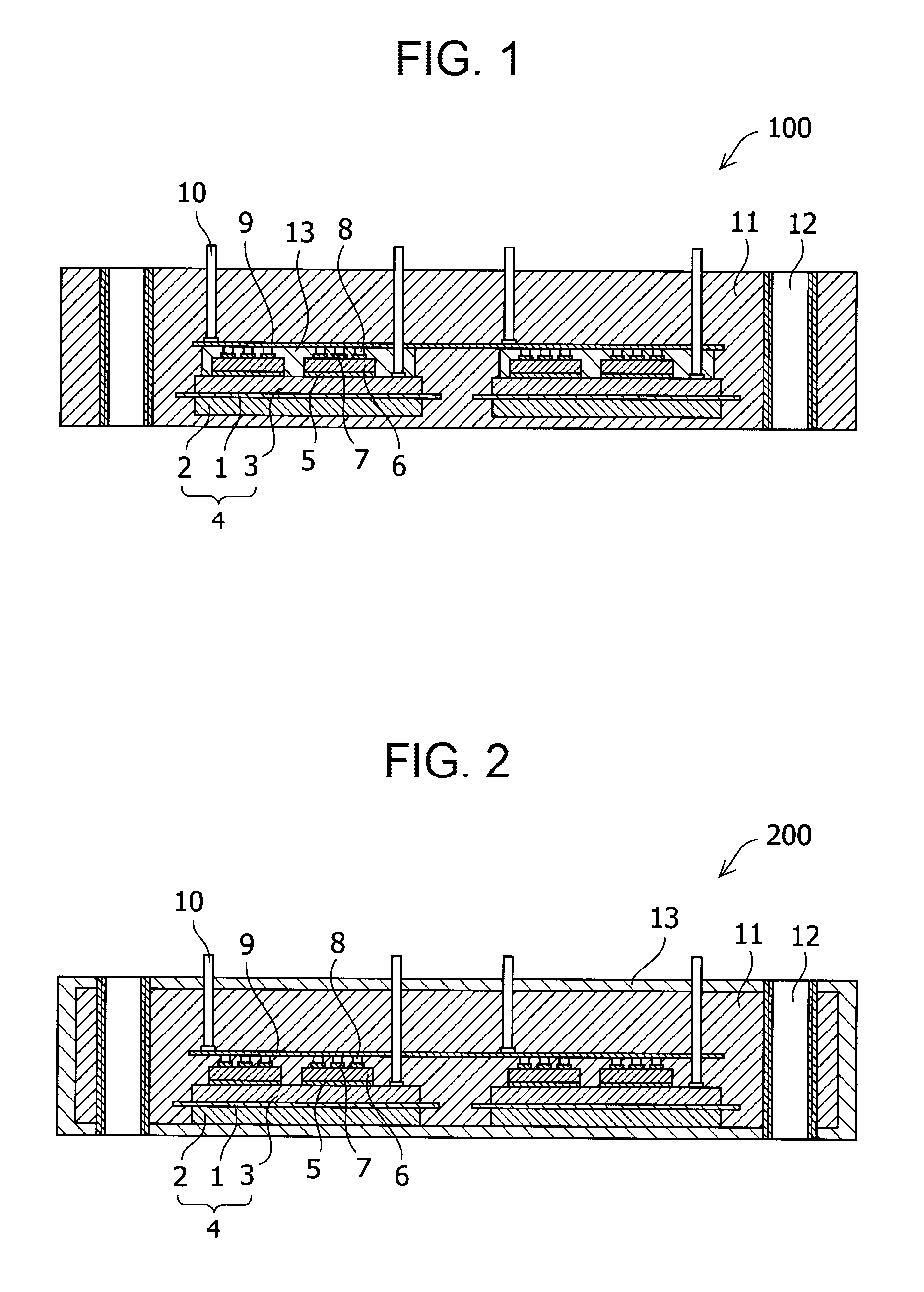
[0049]According to a second embodiment of the invention, a semiconductor device includes a molded body that is obtained by sealing, with a sealing material, a member including a semiconductor element, an insulating substrate which is bonded to one surface of the semiconductor element, and a printed circuit board which is used for a connection to an external circuit and is bonded to the other surface of the semiconductor element. A second sealing material which is a thermosetting resin or a thermoplastic resin forms a first sealing layer that covers the semiconductor element. A first sealing material which is a nanocomposite resin forms a second sealing layer that covers the first sealing layer, faces at least a portion of an outer surface of the molded body, and is provided with at least a thickness of 300 μm.

[0050]FIG. 2 is a diagram illustrating the cross-sectional structure of a semiconductor module molded structure 200 which is an example of a semiconductor device according to t...

third embodiment

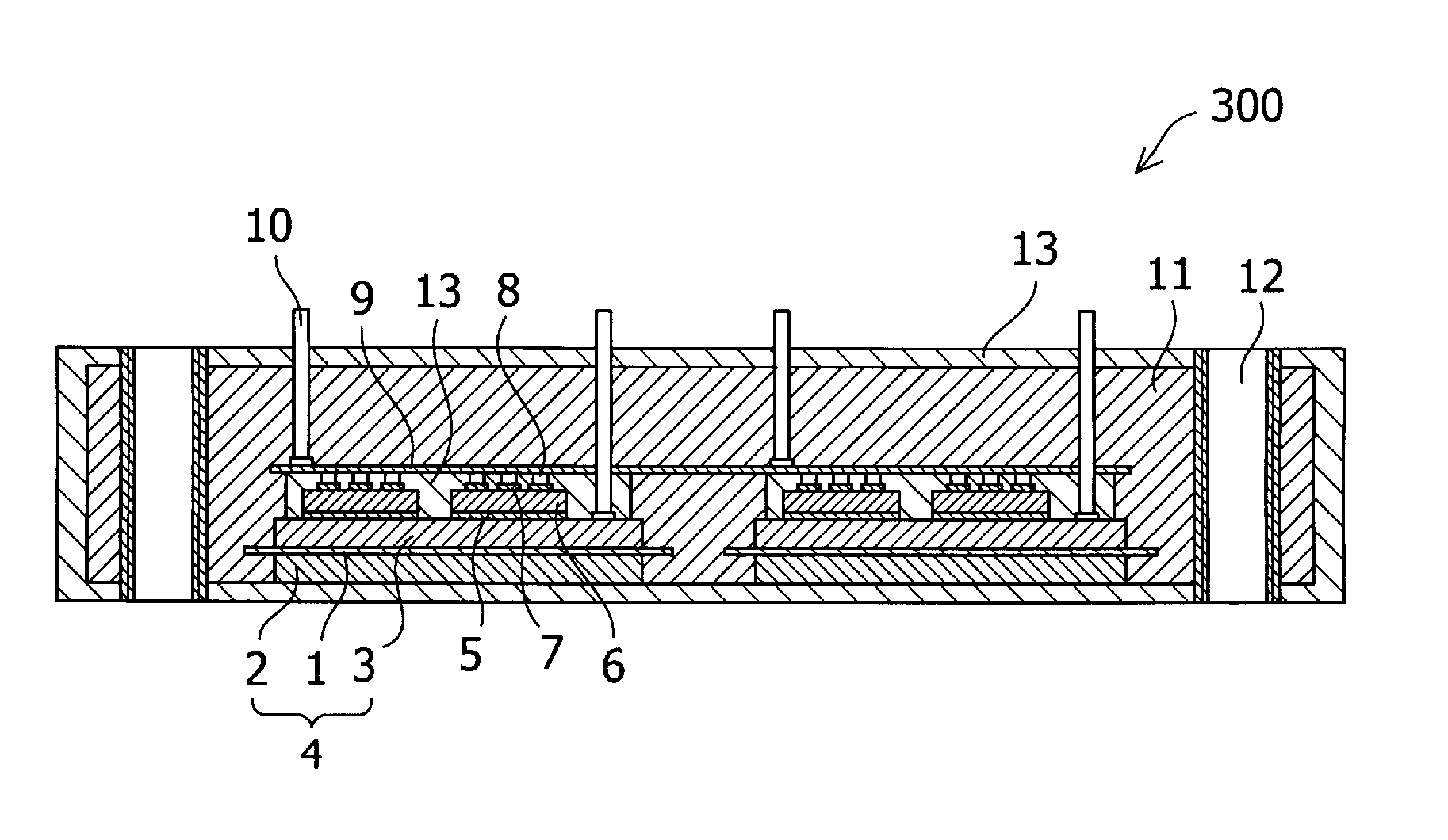
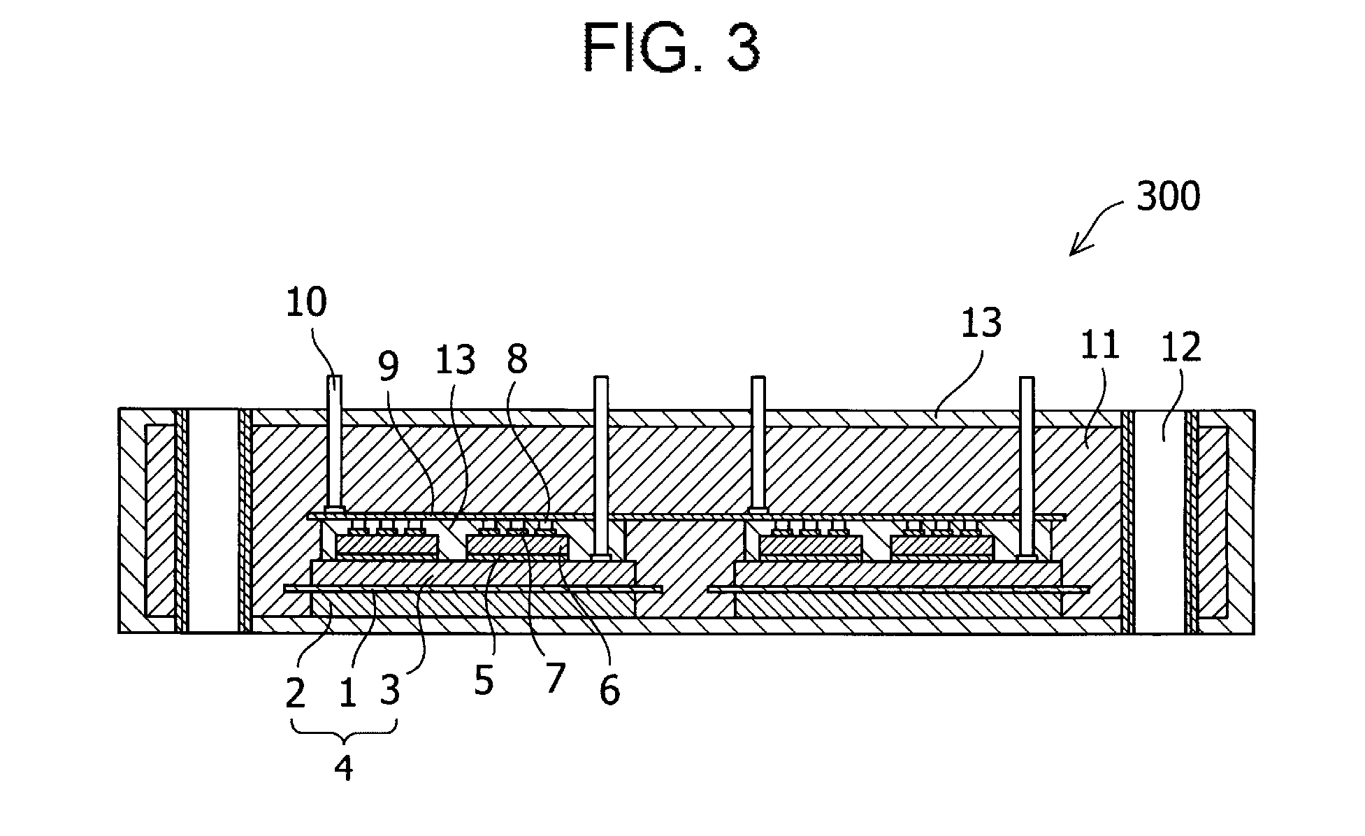
[0059]According to a third embodiment of the invention, a semiconductor device includes a molded body that is obtained by sealing, with a sealing material, a member including a semiconductor element, an insulating substrate which is bonded to one surface of the semiconductor element, and a printed circuit board which is used for a connection to an external circuit and is bonded to the other surface of the semiconductor element. A first sealing material which is a nanocomposite resin forms a first sealing layer that covers the semiconductor element and is provided in a region adjacent to the semiconductor element. A second sealing material which is a thermosetting resin or a thermoplastic resin forms a second sealing layer that covers the first sealing material. The first sealing material which is the nanocomposite resin forms a third sealing layer that further covers the second sealing material, faces at least a portion of an outer surface of the molded body, and is provided with at...


PUM

PropertyMeasurementUnit
particle sizeaaaaaaaaaa
operating temperatureaaaaaaaaaa
thicknessaaaaaaaaaa

Abstract

A semiconductor device includes a molded body obtained by sealing, with a sealing material, a member including a semiconductor element, an insulating substrate which is bonded to one surface of the semiconductor element, and a printed circuit board which is used for a connection to an external circuit and is bonded to another surface of the semiconductor element. The sealing material includes a first sealing material which is a nanocomposite resin including an epoxy base resin, a curing agent, and an inorganic filler with an average particle size of 1 nm to 100 nm; and a second sealing material which is a thermosetting resin, a thermoplastic resin, or a mixture thereof without an inorganic filler. The sealing material is less likely to be degraded by thermal oxidation, even when the semiconductor element operates at a high temperature of 175° C. or higher, is crack resistant, and has high reliability and durability.

Description

CROSS-REFERENCE TO RELATED APPLICATIONS[0001]This non-provisional application for a U.S. patent is a Continuation of International Application PCT / JP2014 / 069813 filed Jul. 28, 2014, which claims priority from JP PA 2013-190787 filed Sep. 13, 2013, the entire contents of both of which are hereby incorporated by reference.BACKGROUND OF THE INVENTION[0002]1. Field of the Invention[0003]The present invention relates to a semiconductor element sealing material, and more particularly, to a semiconductor device using silicon carbide (SiC) or gallium nitride (GaN).[0004]2. Background of the Related Art[0005]In a semiconductor device using a silicon (Si) semiconductor element which has been generally used, sealing has been performed with epoxy resin or silicon gel to ensure insulation. SiC or GaN has better electrical characteristics than Si. Therefore, in recent years, research and development for putting the SiC or GaN semiconductor element to practical use have been conducted. The SiC or ...

Claims


Application Information

Patent Timeline
Patent Type & Authority Patents(United States)
IPC IPC(8): H01L23/48H01L29/16H01L23/29H01L25/07H01L25/18H01L23/31H01L23/00H01L23/28
CPCH01L23/295H01L23/3135H01L24/01H01L25/07H01L25/18H01L29/1608H01L23/28H01L23/293H01L2924/351H01L2924/00
Inventor TAKEMATSU, YUJIYANAGAWA, KATSUHIKOOKAMOTO, KENJI
Owner FUJI ELECTRIC CO LTD
Why Eureka
Try Eureka