Conductive film and touch panel including the same

a technology of conductive film and touch panel, which is applied in the direction of printed circuit aspects, instruments, metallic pattern materials, etc., can solve the problems of limiting the improvement of the properties of an electronic device including indium-tin oxide, the cost of materials such as indium-tin oxide, and the inability to achieve high production efficiency of vacuum deposition methods, so as to improve the hardness of the conductive film, prevent the damage of the conductive layer or the change of properties of the conductive layer

Active Publication Date: 2016-10-04
LG CHEM LTD
View PDF26 Cites 1 Cited by
  • Summary
  • Abstract
  • Description
  • Claims
  • Application Information

AI Technical Summary

Benefits of technology

[0013]The conductive film may include the first hard coating layer formed between the conductive layer (including conductors of nano-materials having a network structure) and the base member. As a result, hardness of the conductive film may be improved, thereby preventing damage of the conductive layer or change of properties thereof during a process. Additionally, the surface on which the conductive layer is formed may be planarized, thereby improving coating properties of the conductive layer and reducing scattered reflection.
[0014]The touch panel may include the conductive layer including a plurality of conductors composed of a nano-material having a network structure. As a result, the conductive layer may include a non-conductive portion, thereby improving transmittance, reducing cost due to decrease in amount of raw materials used for the conductors and obtaining low resistance due to superior electrical properties of the conductors. Accordingly, the touch panel may include the conductive layer, which has a lower resistance and a smaller thickness than other portions touch panel, and thus may be implemented in a wider area and exhibit superior optical properties and / or the like.

Problems solved by technology

However, the material (such as indium-tin oxide) may be expensive and the method of vacuum deposition does not have high production efficiency.
Additionally, there may be a limit in improving properties of an electronic device including indium-tin oxide because the indium-tin oxide is not flexible and may have a high resistance.

Method used


Image

  • Conductive film and touch panel including the same
  • Conductive film and touch panel including the same
  • Conductive film and touch panel including the same

Examples


Embodiment Construction

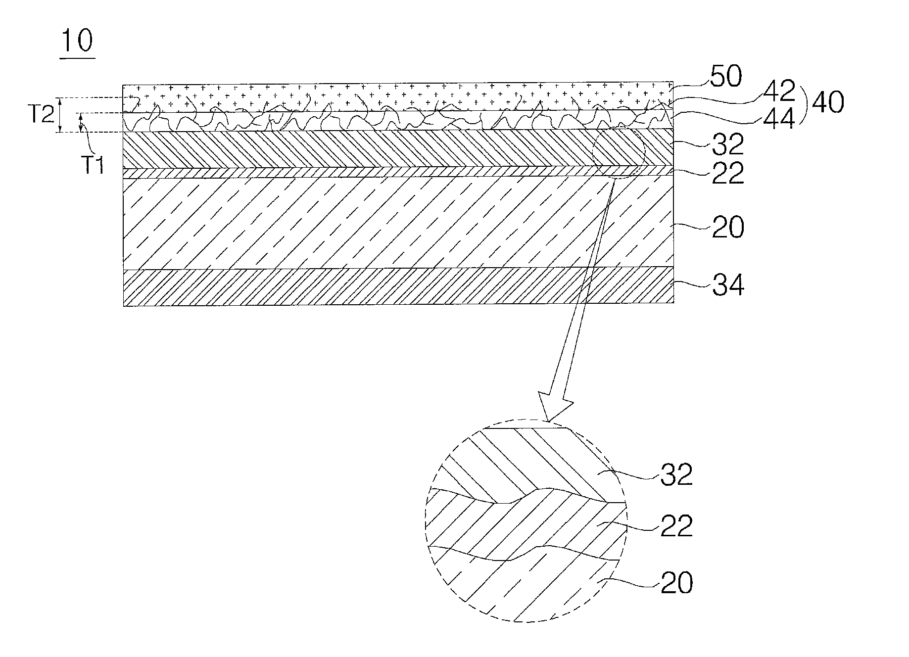
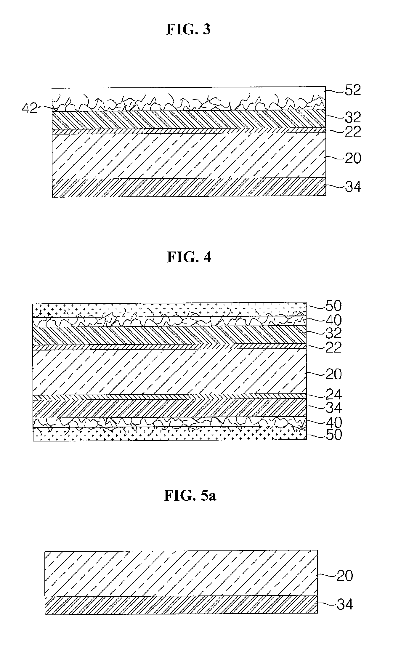
[0035]Reference may be made in detail to the preferred embodiments, examples of which are illustrated in the accompanying drawings. Embodiments are not limited to the disclosed embodiments and embodiments may be modified into various forms.

[0036]In the drawings, parts unrelated to the description may not be illustrated for clear and brief description, and same reference numbers may be used throughout the specification to refer to the same or considerably similar parts. In the drawings, thickness or size may be exaggerated or reduced for more clear description. In addition, the size or area of each constituent element may not be limited to that illustrated in the drawings.

[0037]It will be further understood that, throughout this specification, when one element is referred to as “comprising” another element, the term “comprising” specifies the presence of another element but does not preclude the presence of other additional elements, unless context clearly indicates otherwise. Additi...


PUM


Abstract

A conductive film may be provided that includes a base member, a first hard coating layer formed on a surface of the base member, and a conductive layer formed on the first hard coating layer. The conductive layer may include conductors composed of a nano-material forming a network structure.

Description

CROSS-REFERENCE TO RELATED APPLICATIONS[0001]This application claims the priority benefit of Korean Patent Applications Nos. 2013-0071082 and 2013-0083023 filed on Jun. 20, 2013 and Jul. 15, 2013, respectively, in the Korean Intellectual Property Office, the subject matters of which are incorporated herein by reference.BACKGROUND[0002]1. Field[0003]Embodiments may relate to a conductive film and a touch panel including a conductive film.[0004]2. Background[0005]A portable terminal may have one or more of voice and video calling function, information input and output function and data storage memory function. A portable terminal may have complicated functions such as photographing of images or videos, playing of music files or video files, games, broadcasting and wireless internet and may be implemented as a general multimedia player.[0006]The portable terminal may wirelessly access the Internet, thus enabling web surfing, talk with friends or colleagues via access to a messenger, tr...

Claims


Application Information

Patent Timeline
Patent Type & Authority Patents(United States)
IPC IPC(8): G06F3/044H05K1/09
CPCG06F3/044G06F2203/04112H05K1/097G06F3/0446G06F3/041G06F2203/04103H05K2201/026
Inventor KIM, YUHEEHUR, YANGWOOKCHOI, JINYOUNGLEE, MUNSU
Owner LG CHEM LTD
Why Eureka
Try Eureka