Thin film transistor array substrate and organic light-emitting display device including the same

a technology of thin film transistors and array substrates, applied in semiconductor devices, instruments, electrical devices, etc., can solve the problems of ensuring the life span of pixels by approaching the limit, and achieve the effect of the aperture ratio of the unit pixel

Active Publication Date: 2016-10-25
SAMSUNG DISPLAY CO LTD
View PDF34 Cites 16 Cited by
  • Summary
  • Abstract
  • Description
  • Claims
  • Application Information

AI Technical Summary

Benefits of technology

[0008]Aspects of the present invention provide a high resolution organic light-emitting display device for improving a life span of the display by reducing a space limitation of via holes that are factors (e.g., critical factors) when designing a high resolution pixel.

Problems solved by technology

While high resolution pixels for the high resolution display may be required, openings of a pixel definition layer for ensuring a life span of pixels are approaching a limit due to a design constraint (or rule) of a metal wiring in the pixel and a gap between the pixel definition layers, that is, the restriction of a margin for deposition using a fine metal mask (FMM).

Method used


Image

  • Thin film transistor array substrate and organic light-emitting display device including the same
  • Thin film transistor array substrate and organic light-emitting display device including the same
  • Thin film transistor array substrate and organic light-emitting display device including the same

Examples


Embodiment Construction

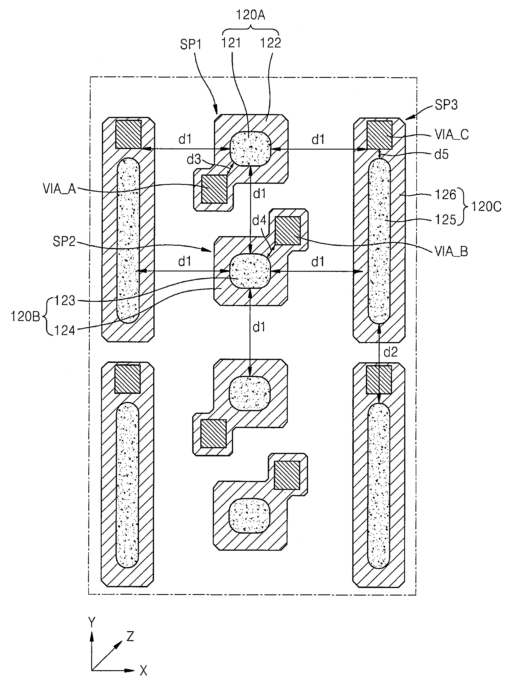
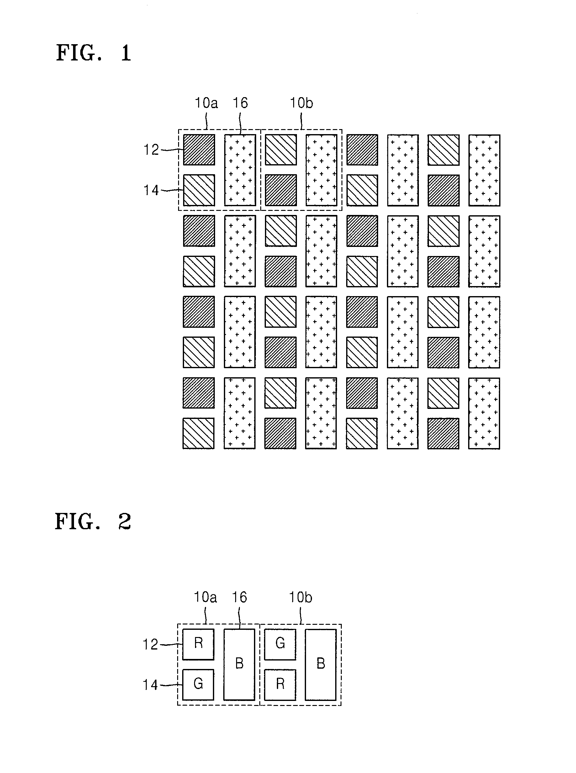
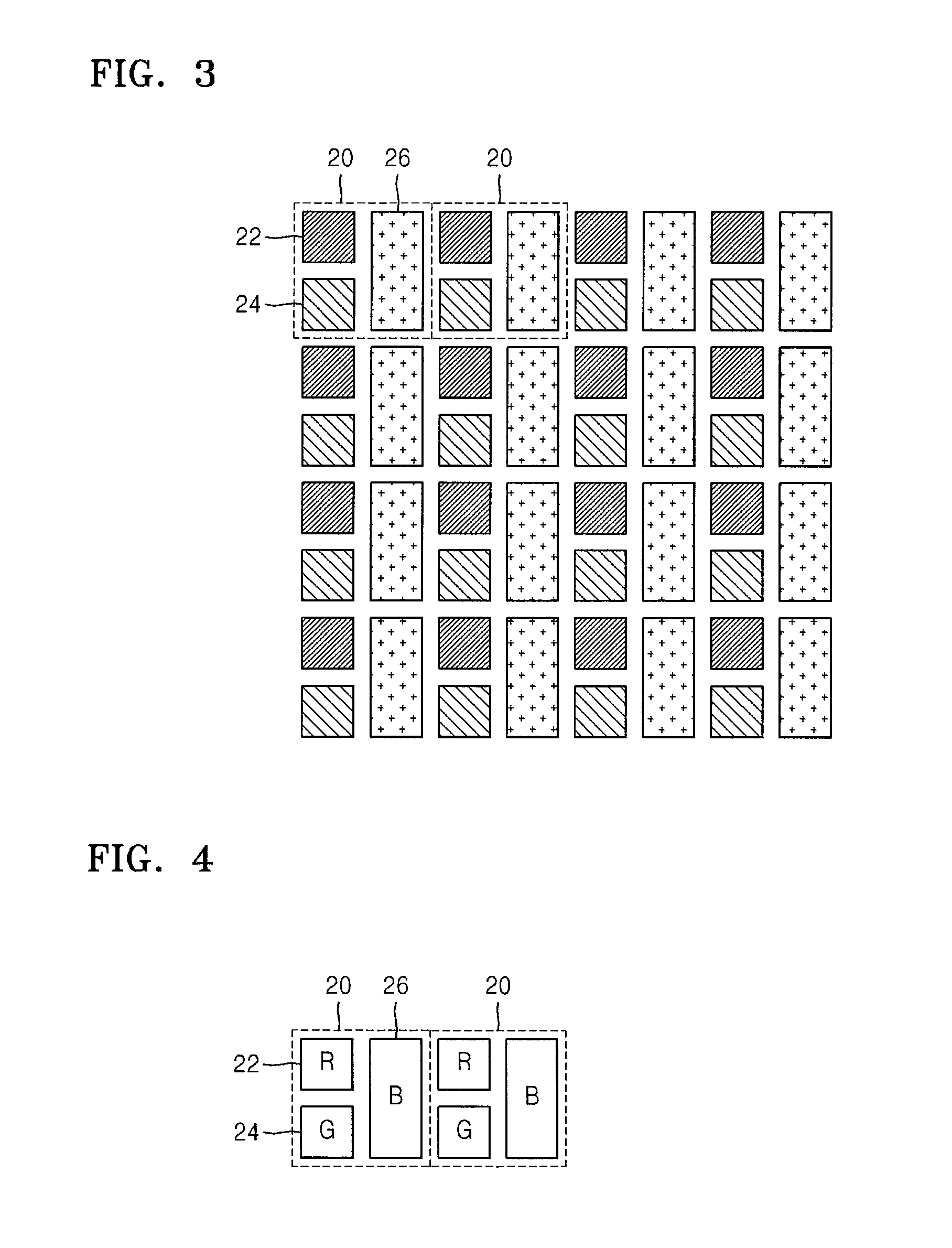
[0044]Hereinafter, embodiments of the present invention will be described in detail by explaining example embodiments of the invention with reference to the attached drawings. The invention may, however, be embodied in many different forms, and should not be construed as being limited to the embodiments set forth herein; rather, these embodiments are provided so that this disclosure will be more thorough and complete, and will more fully convey the concept of the invention to those skilled in the art.

[0045]In the following description, well-known functions or constructions may not be described in detail since they would obscure the invention with unnecessary detail, and like reference numerals in the drawings denote like or similar elements throughout the specification.

[0046]Also, the thicknesses and sizes of elements in the drawings may be arbitrarily shown for convenience of description, thus, the spirit and scope of the present invention are not necessarily defined by the drawing...


PUM


Abstract

A thin film transistor array substrate having a pixel arrangement structure includes a first sub-pixel for displaying a first color and a second sub-pixel for displaying a second color alternately located in a first column, and a third sub-pixel for displaying a third color in a second column adjacent to the first column, and via holes of the first through third sub-pixels in a same row are at different positions.

Description

CROSS-REFERENCE TO RELATED PATENT APPLICATION[0001]This application claims priority to and the benefit of Korean Patent Application No. 10-2013-0033085, filed on Mar. 27, 2013, in the Korean Intellectual Property Office, the disclosure of which is incorporated herein in its entirety by reference.BACKGROUND[0002]1. Field[0003]The present invention relates to a thin film transistor array substrate and an organic light-emitting display device including the same.[0004]2. Description of Related Art[0005]An organic light-emitting display device is self-emissive, and unlike a liquid crystal display device, the organic light-emitting display device does not require a separate light source, thereby having a reduced thickness and weight. Also, the organic light-emitting display device has beneficial characteristics including low power consumption, high brightness, a quick response time, or the like.[0006]In general, the organic light-emitting display device includes gate lines that are dispos...

Claims


Application Information

Patent Timeline
Patent Type & Authority Patents(United States)
IPC IPC(8): H01L27/32G09G3/32H01L27/12
CPCH01L27/3216G09G3/3233H01L27/3218G09G2300/0452G09G2300/0465G09G2300/0819G09G2310/0262H01L27/124H10K59/352H10K59/353H10K59/121H10K59/1213H10K59/1216H10K59/122H10K59/131H10K59/123H10K59/124
Inventor LEE, WON-SE
Owner SAMSUNG DISPLAY CO LTD
Why Eureka
Try Eureka