Supercharge Your Innovation With Domain-Expert AI Agents!

Light emitting diode chip, light emitting device, and wafer-level structure of light emitting diode

a technology of light emitting diodes and led chips, which is applied in the direction of basic electric elements, electrical equipment, semiconductor devices, etc., to achieve the effect of improving light output efficiency and uniformity of light output of led chips

Active Publication Date: 2016-11-22
EPISTAR CORP
View PDF14 Cites 0 Cited by
  • Summary
  • Abstract
  • Description
  • Claims
  • Application Information

AI Technical Summary

Benefits of technology

The patent text describes a light emitting device that has a specific design to prevent delamination between the encapsulant and the growing base, which increases its reliability. This device also has improved light output and efficiency due to its unique structure. The text also mentions a wafer-level structure where multiple light emitting diode chips can be fabricated on a growing substrate, saving cost and improving yield. Additionally, the text discusses the use of an encapsulant that can be tightly fixed to the growing base, preventing delamination and improving the overall performance of the device.

Problems solved by technology

Since sapphire is a transparent material, an LED chip fabricated by using sapphire would scatter light to all directions without focusing the light and resulting in waste.

Method used


Image

  • Light emitting diode chip, light emitting device, and wafer-level structure of light emitting diode
  • Light emitting diode chip, light emitting device, and wafer-level structure of light emitting diode
  • Light emitting diode chip, light emitting device, and wafer-level structure of light emitting diode

Examples


Embodiment Construction

[0023]Reference will now be made in detail to the present preferred embodiments of the application, examples of which are illustrated in the accompanying drawings.

[0024]Wherever possible, the same reference numbers are used in the drawings and the description to refer to the same or like parts.

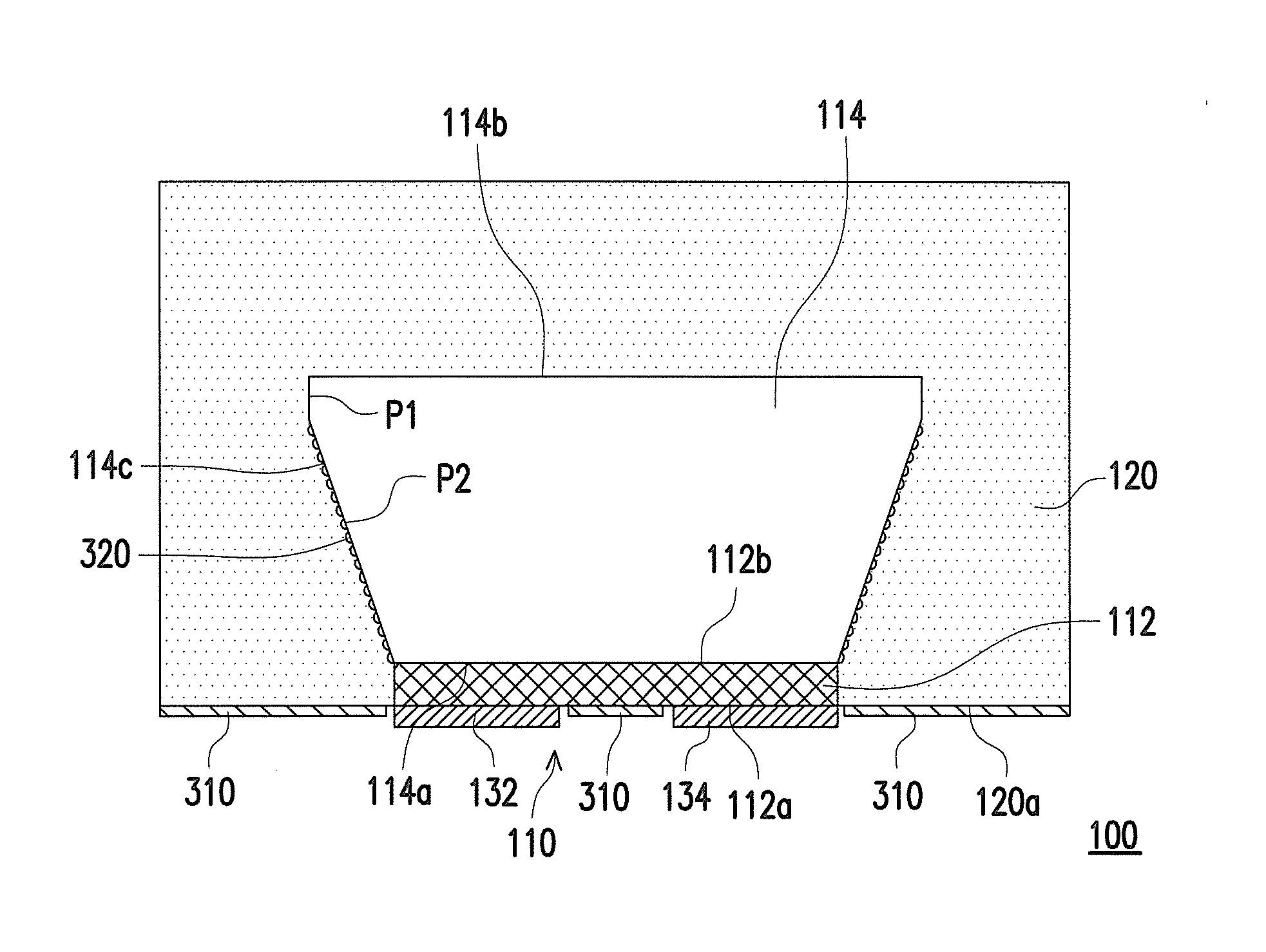
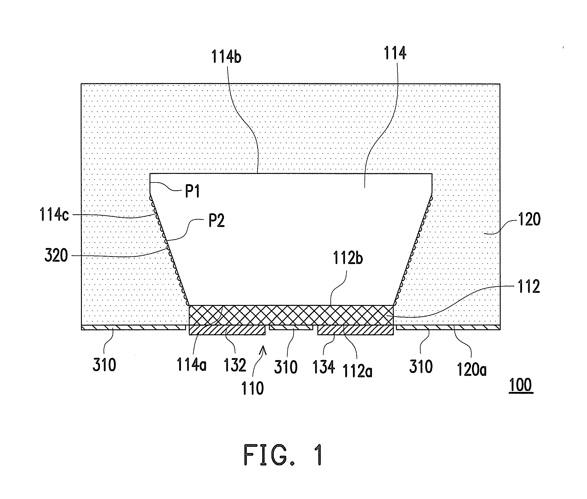
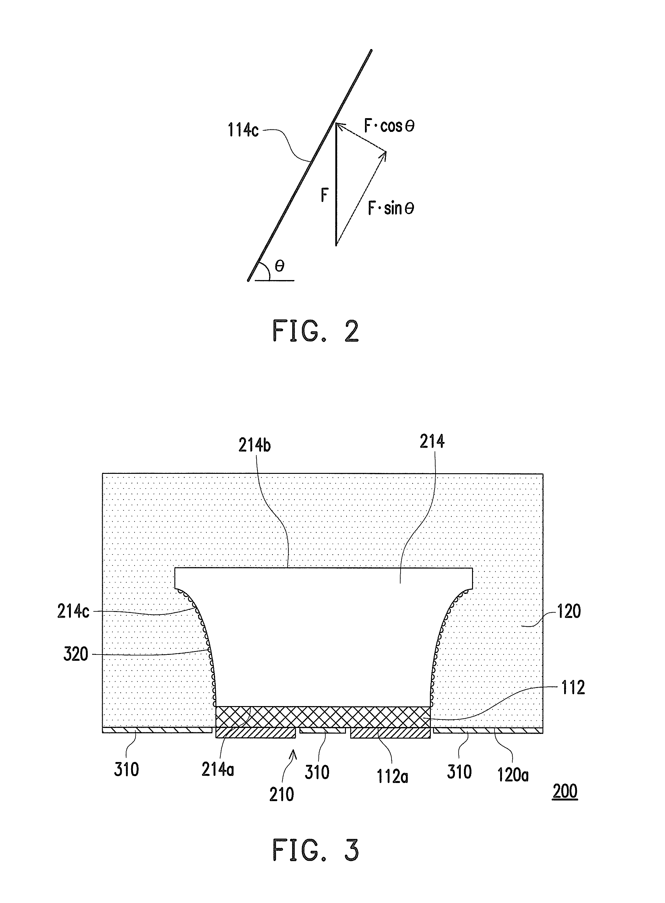
[0025]FIG. 1 illustrates a light emitting device 100 according to an embodiment of the present application. The light emitting device 100 can be formed by packaging an LED chip 110 with an encapsulant 120. The encapsulant 120 may comprise phosphors. The LED chip 110 comprises an LED structure layer 112 having a first surface 112a and a second surface 112b opposite to the first surface 112a, which can be formed on a growing base 114.

[0026]In the present embodiment, the growing base 114 is not removed after performing the manufacturing of the LED structure layer. The growing base 114 may be a sapphire substrate or other applicable substrate. The LED structure layer 112 is essentially formed from...


PUM


Abstract

A light emitting device is provided with a growing base having specific geometry to prevent delamination between the encapsulant and the growing base, and thereby enhance structural reliability of the light emitting device. Furthermore, the light emitting efficiency as well as uniformity of light output of the light emitting device can be improved by forming the side surface of the growing base with at least a curved portion or slanted portion, and uneven structures can be formed on the curved portion or slanted portion to further improve the uniformity of light output. Furthermore, the light emitting diode chips can be fabricated by taking batch processing on the growing substrate, as provided in the wafer-level structure, with the advantages of saving cost, improving yield, etc.

Description

CROSS-REFERENCE TO RELATED APPLICATION[0001]This application claims the priority benefits of U.S. provisional application Ser. No. 62 / 007,419, filed on Jun. 4, 2014. The entirety of the above-mentioned patent application is hereby incorporated by reference herein and made a part of this specification.BACKGROUND[0002]1. Field of the Invention[0003]The present application relates to a light emitting diode (LED) chip, a light emitting device, and a wafer-level structure of light emitting diode.[0004]2. Description of Related Art[0005]An LED chip is a semiconductor element constituted mainly by, for example, group III-V compound semiconductor materials. Since such semiconductor materials have a characteristic of converting electricity into light, when a current is applied to the semiconductor materials, electrons therein are combined with holes and excessive energy are released in form of light, thereby achieving an effect of luminosity.[0006]Sapphire is often used as an epitaxial subst...

Claims


Application Information

Patent Timeline
Patent Type & Authority Patents(United States)
IPC IPC(8): H01L29/06H01L21/00H01L33/20H01L33/60
CPCH01L33/20H01L33/60
Inventor CHEN, CHUN-WEILI, JEN-CHIHPAN, SHYI-MING
Owner EPISTAR CORP
Features
  • R&D
  • Intellectual Property
  • Life Sciences
  • Materials
  • Tech Scout
  • Unparalleled Data Quality
  • Higher Quality Content
  • 60% Fewer Hallucinations
Learn More