Self repair device and method thereof

Active Publication Date: 2016-11-29
SK HYNIX INC
View PDF8 Cites 60 Cited by
  • Summary
  • Abstract
  • Description
  • Claims
  • Application Information

AI Technical Summary

Benefits of technology

[0019]According to the embodiments, the self repair device and method may select the row or column redundancy according to various types of defects w

Problems solved by technology

The decrease in the design rule may increase the probability of defects in the semiconductor memory devices, and one or more defects in a chip may cause the chip to be discarded.
Thus, when a column-based defect occurs, the yield may decrease because the column-based defect cannot be repaired.
During a package-level test, a bit failure, a row

Method used


Image

  • Self repair device and method thereof
  • Self repair device and method thereof
  • Self repair device and method thereof

Examples


Embodiment Construction

[0026]Hereinafter, a self repair device and method will be described below with reference to the accompanying drawings through various examples of embodiments.

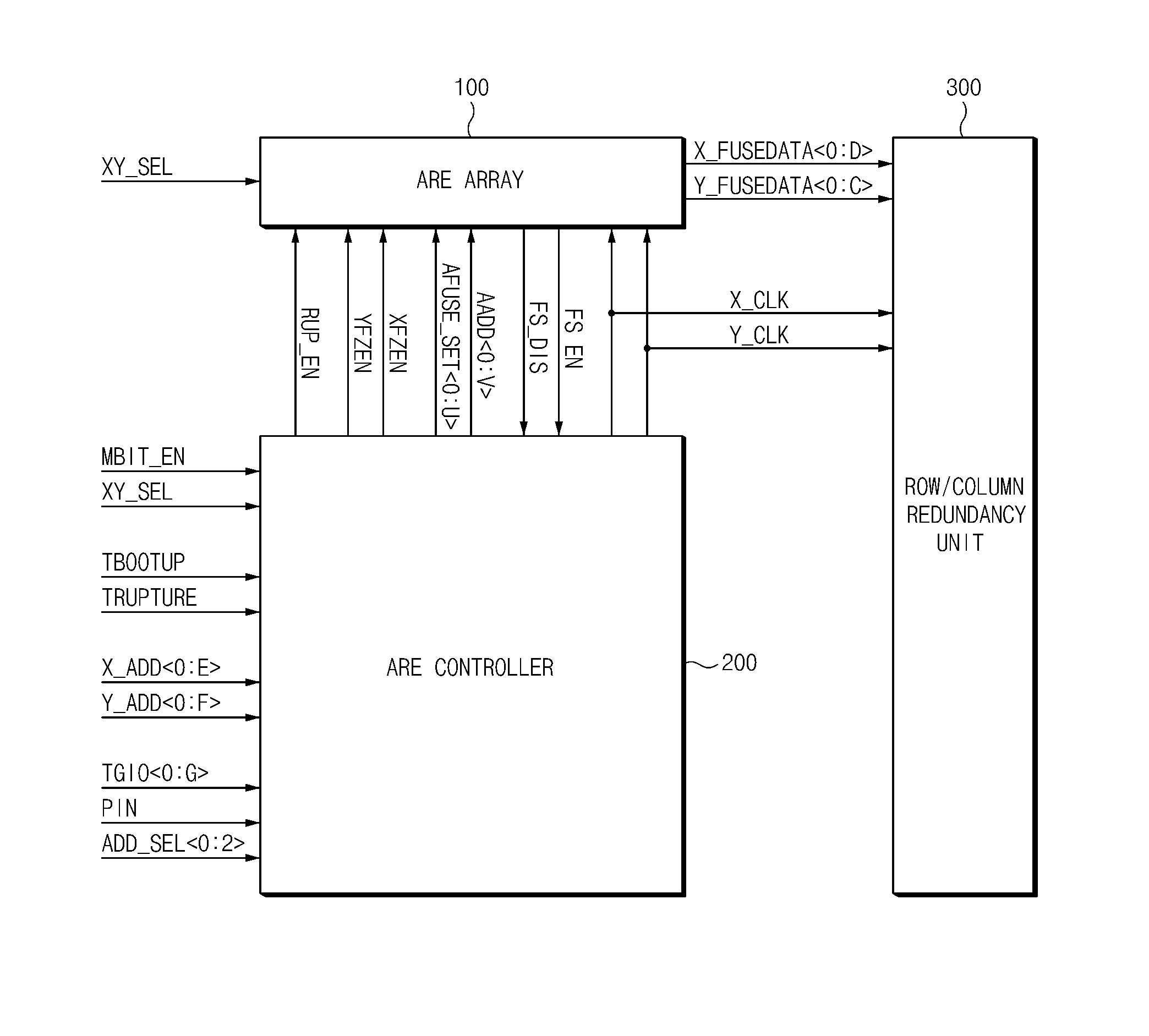
[0027]FIG. 1 is a configuration diagram of a self repair device in accordance with an embodiment. In an embodiment, a semiconductor memory device may include the self repair device.

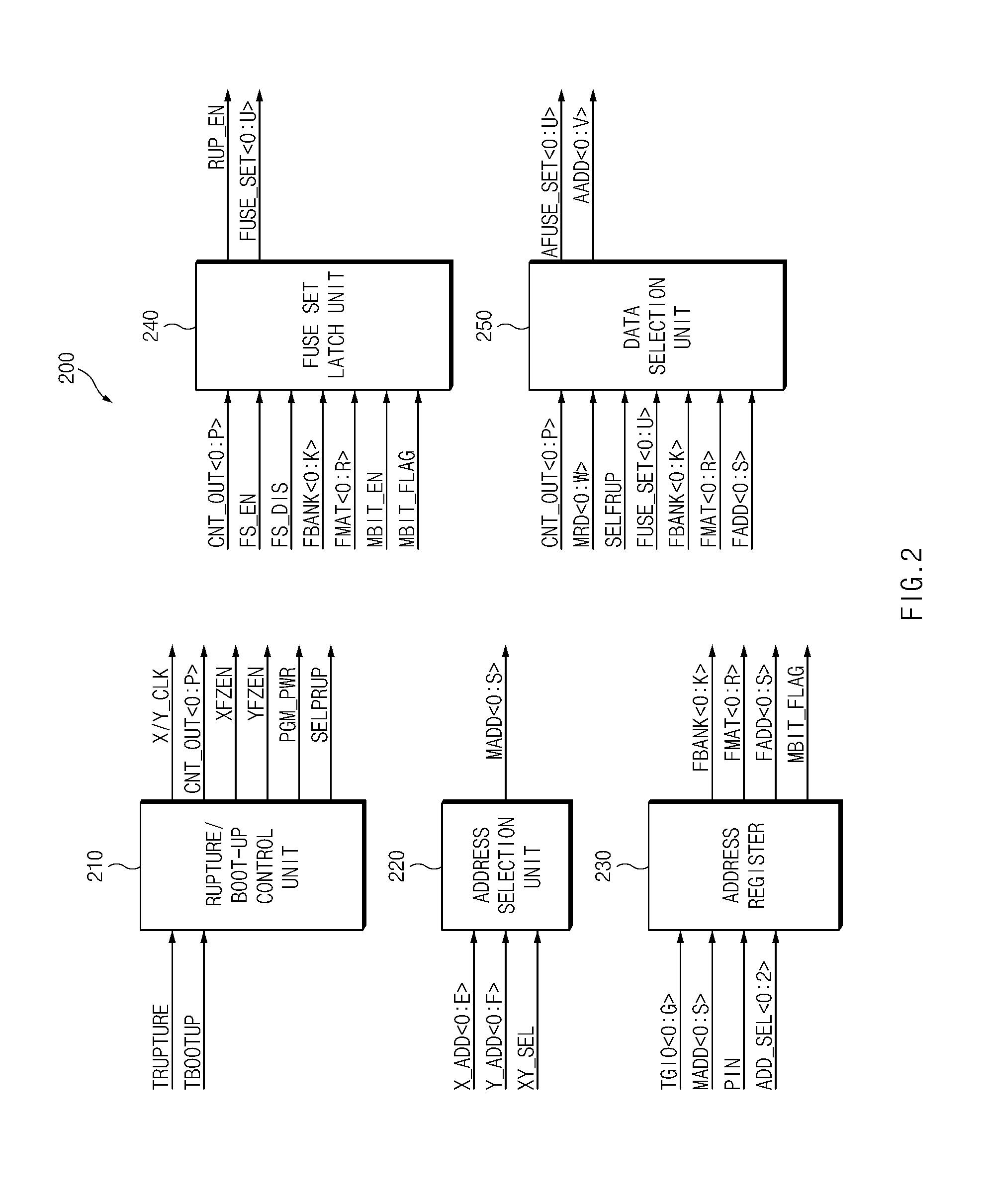
[0028]The self repair device in accordance with an embodiment may include an Array Rupture Electrical fuse (hereinafter referred to as “ARE”) array 100, an ARE controller 200, and a row / column redundancy unit 300.

[0029]The ARE array 100 may store information on the address that a failure has occurred. Such information collected during a memory test may be temporarily stored in a storage device of memory tester, and then applied the semiconductor memory device to rupture electrical fuses corresponding to the respective address in order to permanently store the information at the semiconductor memory device.

[0030]The ARE array 100 may receive a fuse s...


PUM


Abstract

A self repair device may include: an electrical fuse array configured to store bit information of a failed address in a fuse; an electrical fuse controller configured to store a row address or column address corresponding to a failed bit when a failure occurs, generate a repair address by comparing a failed address inputted during a test to the address stored therein, output a rupture enable signal for controlling a rupture operation of the electrical fuse array, and output row fuse set data or column fuse set data in response to the failed address; and a row/column redundancy unit configured to perform a row redundancy or column redundancy operation in response to the row fuse set data or the column fuse set data applied from the electrical fuse array.

Description

CROSS-REFERENCES TO RELATED APPLICATION[0001]The present application claims priority under 35 U.S.C. §119(a) to Korean application number 10-2015-0085296 filed on Jun. 16, 2015, in the Korean Intellectual Property Office, which is incorporated herein by reference in its entirety.BACKGROUND[0002]1. Technical Field[0003]Various embodiments generally relate to an integrated circuit, and more particularly to a self repair device and method for improving repair efficiency during a package repair operation.[0004]2. Related Art[0005]A semiconductor memory such as Dynamic Random Access Memory (hereinafter referred to as “DRAM”) includes a plurality of memory cells arranged in a matrix. Demands for highly integrated semiconductor memory devices are leading to a decrease in the design rule, which defines the minimum feature size of chip lithography. The decrease in the design rule may increase the probability of defects in the semiconductor memory devices, and one or more defects in a chip ma...

Claims


Application Information

Patent Timeline
IPC IPC(8): G11C17/00G11C29/00G11C17/16G11C17/18
CPCG11C29/78G11C17/16G11C17/18G11C29/76G11C29/4401G11C29/787G11C2029/4402
Inventor SHIM, YOUNG BO
Owner SK HYNIX INC
Why Eureka
Try Eureka