Printed circuit board including electronic component embedded therein and method for manufacturing the same

a technology of printed circuit boards and electronic components, which is applied in the direction of sustainable manufacturing/processing, final product manufacturing, and semiconductor/solid-state device details. it can solve the problems of short circuit, difficult to maximize the flowability of resin leaked from the buildup material in the cavity of the core, and the insufficient mounting area of electronic components. it can improve the reliability and yield of a produ

Active Publication Date: 2016-12-20
SAMSUNG ELECTRO MECHANICS CO LTD
View PDF9 Cites 2 Cited by
  • Summary
  • Abstract
  • Description
  • Claims
  • Application Information

AI Technical Summary

Benefits of technology

[0014]Another object of the present invention is to provide a method for manufacturing a printed circuit board including an electronic component embedded therein, which prevents a lamination of a stacked member to improve reliability and yield of a product.

Problems solved by technology

However, as the size of the board is restricted, a mounting area of electronic components may not be sufficiently secured.
Further, there is a need to make a thickness of the core thick so as to reduce the occurrence of warpage of the board, which makes it difficult to maximize flowability of resin leaked from the buildup material in the space within the cavity of the core.
Further, since a width of the cavity having an electronic component embedded therein is reduced according to a fine pitch of the pattern formed on the printed circuit board, an interval between a side wall of the cavity and the electronic component and when the electronic component is biased to one side within the cavity, electrode patterns formed on the core contacts external electrodes of the electronic component, which leads to a short circuit.

Method used


Image

  • Printed circuit board including electronic component embedded therein and method for manufacturing the same
  • Printed circuit board including electronic component embedded therein and method for manufacturing the same
  • Printed circuit board including electronic component embedded therein and method for manufacturing the same

Examples


Embodiment Construction

[0024]The acting effects and technical configuration with respect to the objects of a printed circuit board including an electronic component embedded therein and a method for manufacturing the same according to the present invention will be clearly understood by the following description in which exemplary embodiments of the present invention are described with reference to the accompanying drawings.

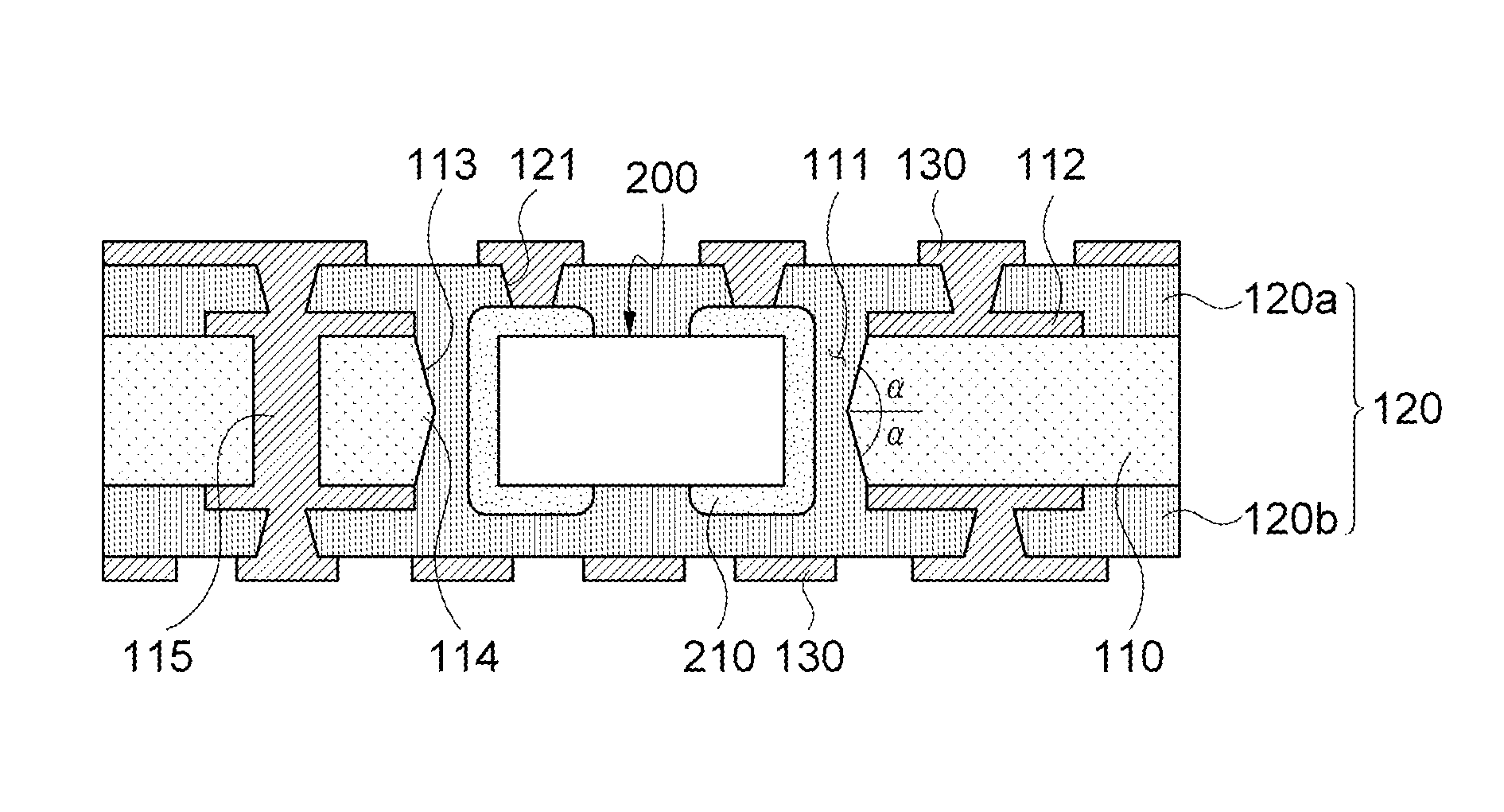
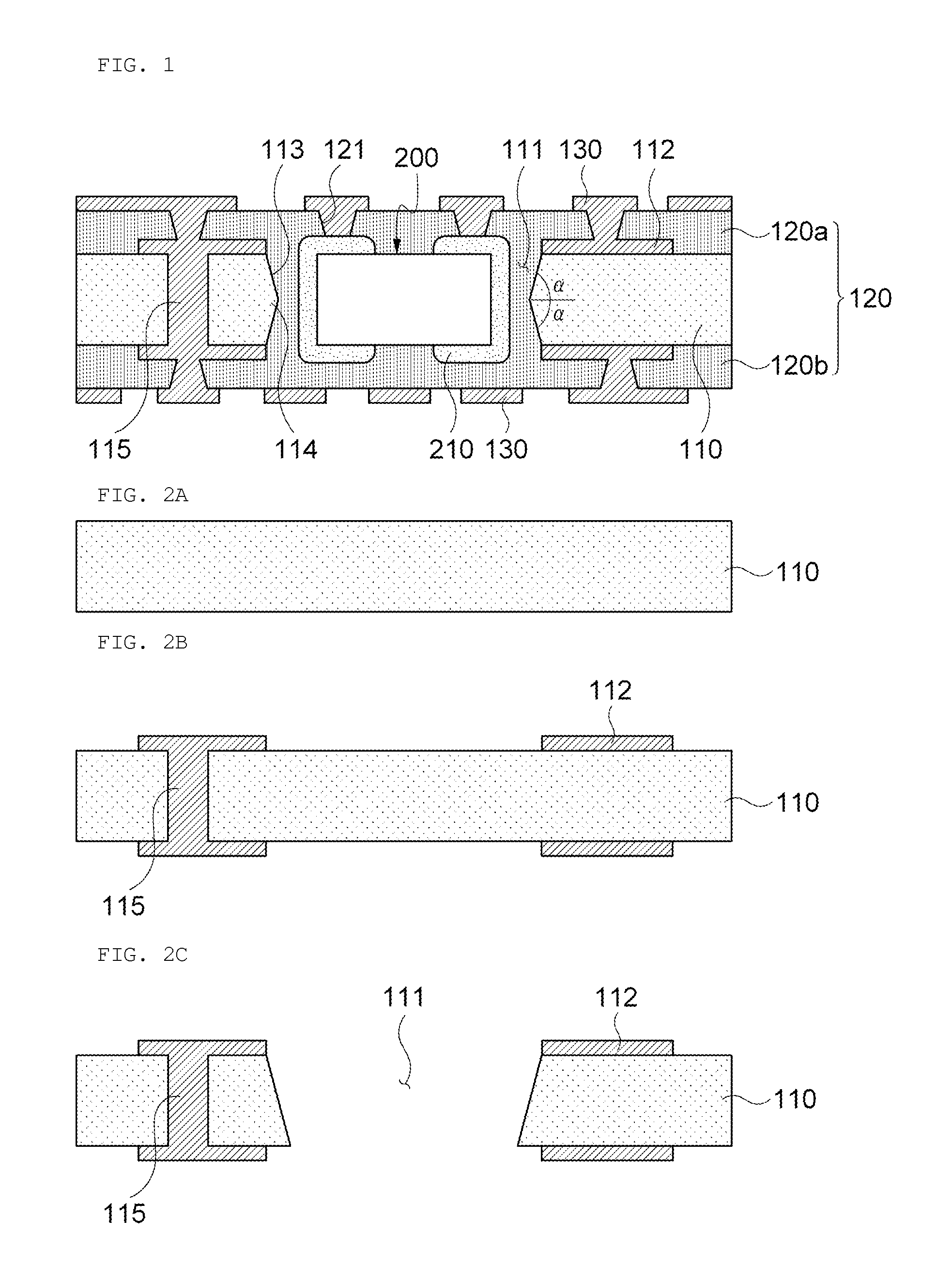
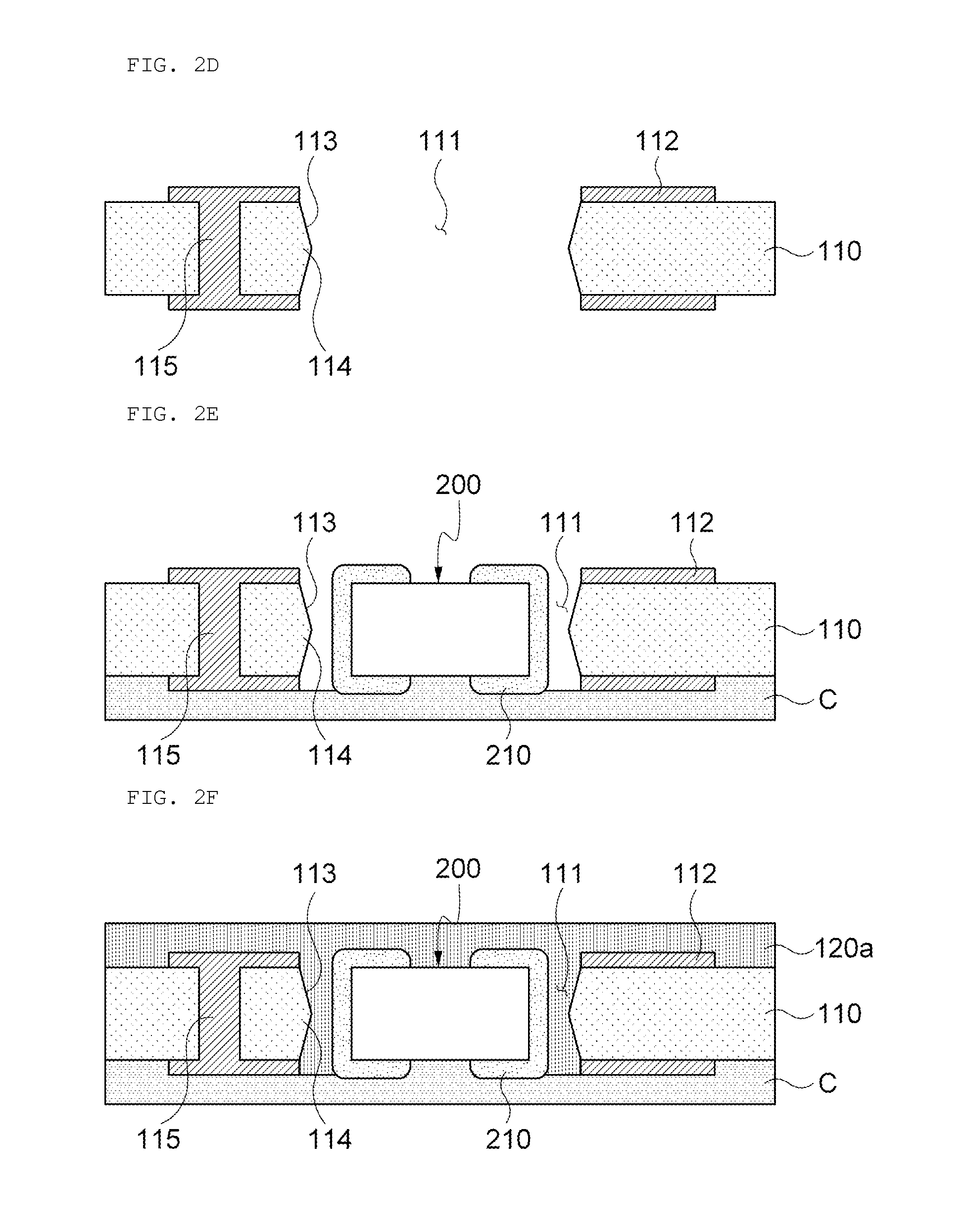
[0025]First, FIG. 1 is a cross-sectional view of a printed circuit board including an electronic component embedded therein according to an exemplary embodiment of the present invention.

[0026]As illustrated in FIG. 1, a printed circuit board 100 including an electronic component embedded therein according to an exemplary embodiment of the present invention may include a core 110 in which a cavity 111 is formed, an electronic component 200 embedded in the cavity 111, an insulating layer 120 stacked on upper and lower portions of the core 110 including the electronic component 200, and ex...


PUM

PropertyMeasurementUnit
micro roughness Raaaaaaaaaaa
insulatingaaaaaaaaaa
acute angleaaaaaaaaaa

Abstract

Disclosed herein are a printed circuit board including an electronic component embedded therein and a method for manufacturing the same. The printed circuit board including an electronic component embedded therein includes: a core formed with a cavity which is formed of a through hole and has a side wall formed with an inclined surface having a top and bottom symmetrically formed based on a central portion thereof; an electronic component embedded in the cavity; insulating layers stacked on upper and lower portions of the core including the electronic component; and external circuit layers formed on the insulating layers.

Description

[0001]This application claims the benefit under 35 U.S.C. Section 119 of Korean Patent Application Serial No. 10-2013-0046733 entitled “Printed Circuit Board Including Electronic Component Embedded Therein And Method For Manufacturing The Same” filed on Apr. 26, 2013, which is hereby incorporated by reference in its entirety into this application.BACKGROUND OF THE INVENTION[0002]1. Technical Field[0003]The present invention relates to a printed circuit board including an electronic component embedded therein and a method for manufacturing the same.[0004]2. Description of the Related Art[0005]As electronic devices, such as cellular phones, IT devices, and the like, are small and light, there is a need to mount electronic components on a restricted area of a board to help the electronic devices perform more functions.[0006]However, as the size of the board is restricted, a mounting area of electronic components may not be sufficiently secured. Therefore, a need exists for a technology...

Claims


Application Information

Patent Timeline
Patent Type & Authority Patents(United States)
IPC IPC(8): H05K1/16H01L23/00H05K1/18H05K3/46H01L21/56
CPCH05K1/185H01L24/19H01L24/20H01L21/568H01L2224/04105H01L2924/12042H05K3/4602H05K2201/09854H05K2201/10636H05K2203/1469Y02P70/611Y10T29/49139H01L2924/00H01L2924/3511Y02P70/50H05K1/18H05K3/46
Inventor LEE, SEUNG EUNCHUNG, YUL KYOSHIN, YEE NALEE, DOO HWAN
Owner SAMSUNG ELECTRO MECHANICS CO LTD
Why Eureka
Try Eureka