Single diffusion break structure and cuts later method of making

Inactive Publication Date: 2017-01-10
GLOBALFOUNDRIES INC
View PDF4 Cites 11 Cited by
  • Summary
  • Abstract
  • Description
  • Claims
  • Application Information

AI Technical Summary

Benefits of technology

[0009]The present invention offers advantages and alternatives over the prior art by providing a structure having an SDB and method of making the same wherein the SDB is less sensitive to lithographic alignment issues. Further the S/D regions adjacent the SDB are substantially equal in volume to S/D regions between pairs of active gates. Additionally, the SDB structure can be scaled down to the 14 nm node and beyond.
[0010]A method of making a structure having a single diffusion break in accordance with one or more aspects of the present invention includes etching rows of fins into a substrate of a structure from a patterned fin hardmask, the remaining fin hardmask being self-aligned with top surfaces of the fins. A first di

Problems solved by technology

With constant down-scaling and increasingly demanding requirements to the speed and functionality of ultra-high density integrated circuits, semiconductor devices, such as transistors, diodes, capacitors and the like, need to continuously reduce space between active (Rx) regions on a semiconductor substrate.
However, as integrated circuits are scaled down to such class sizes as 14 nm node or beyond, the width of a conventional isolation region becomes increasingly problematic as a region devoid of active devices.
However the formation of prior art SDBs probl

Method used


Image

  • Single diffusion break structure and cuts later method of making
  • Single diffusion break structure and cuts later method of making
  • Single diffusion break structure and cuts later method of making

Examples


Example

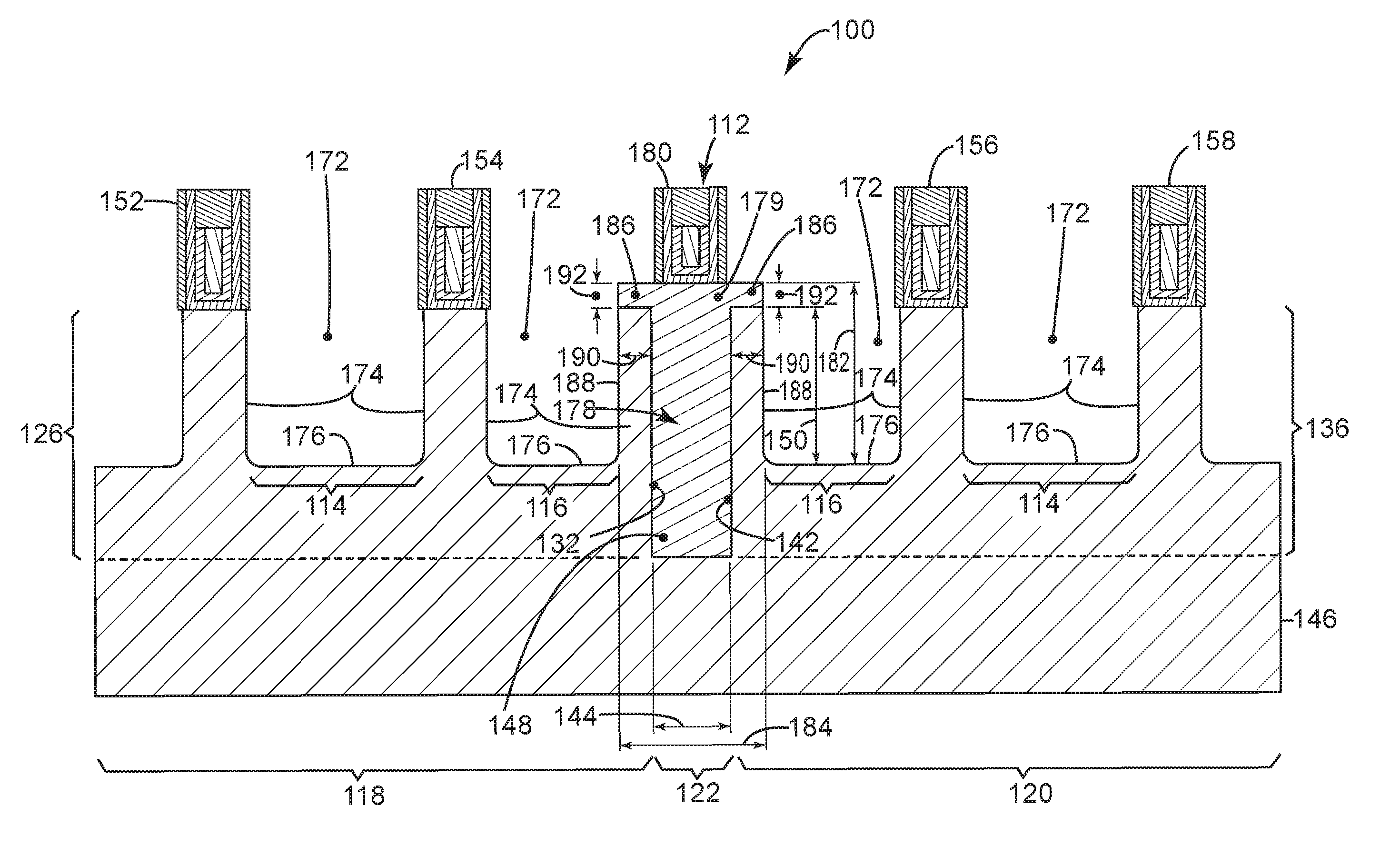
[0061]Certain exemplary embodiments will now be described to provide an overall understanding of the principles of the structure, function, manufacture, and use of the methods, systems, and devices disclosed herein. One or more examples of these embodiments are illustrated in the accompanying drawings. Those skilled in the art will understand that the methods, systems, and devices specifically described herein and illustrated in the accompanying drawings are non-limiting exemplary embodiments and that the scope of the present invention is defined solely by the claims. The features illustrated or described in connection with one exemplary embodiment may be combined with the features of other embodiments. Such modifications and variations are intended to be included within the scope of the present invention.

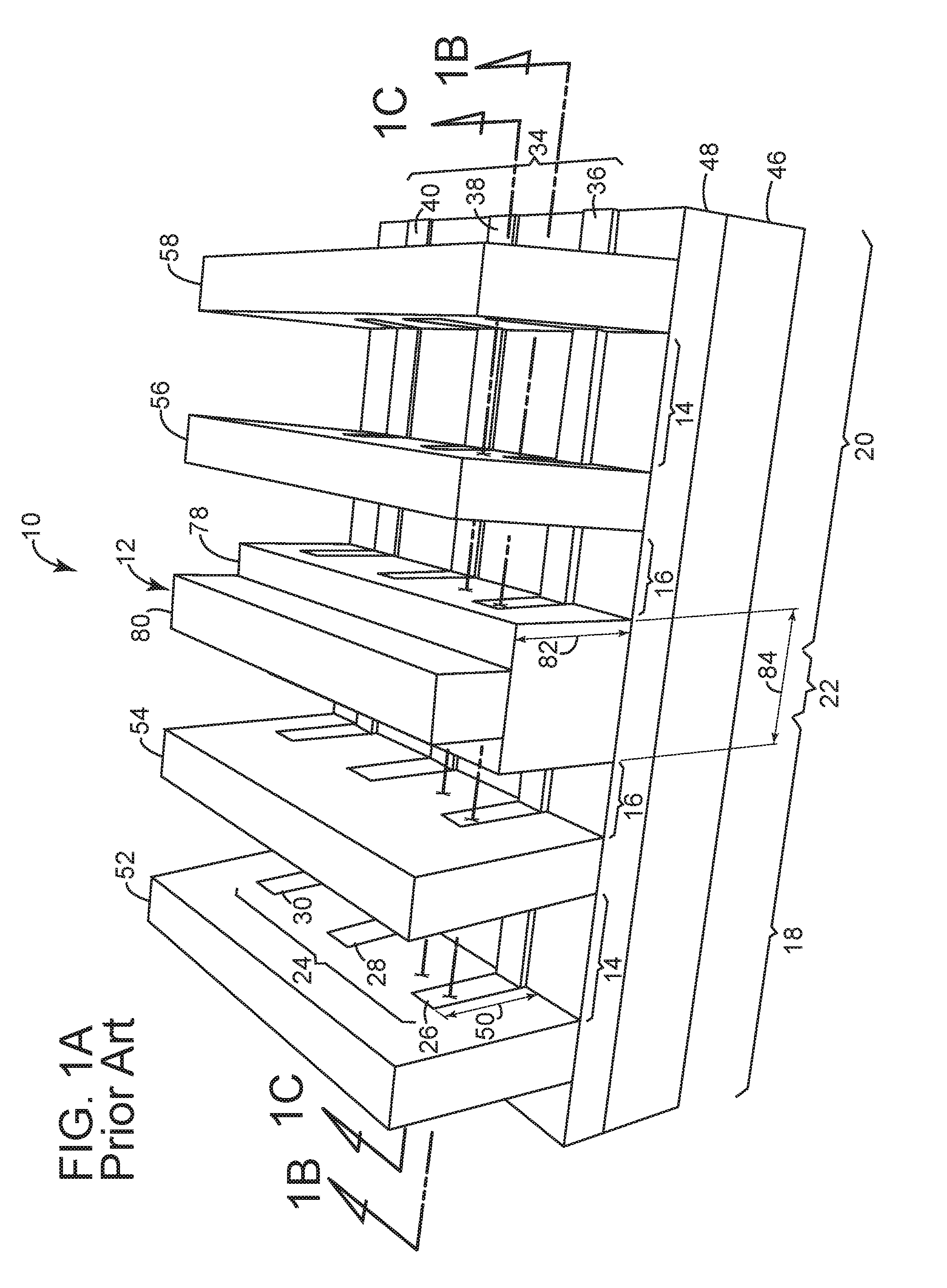
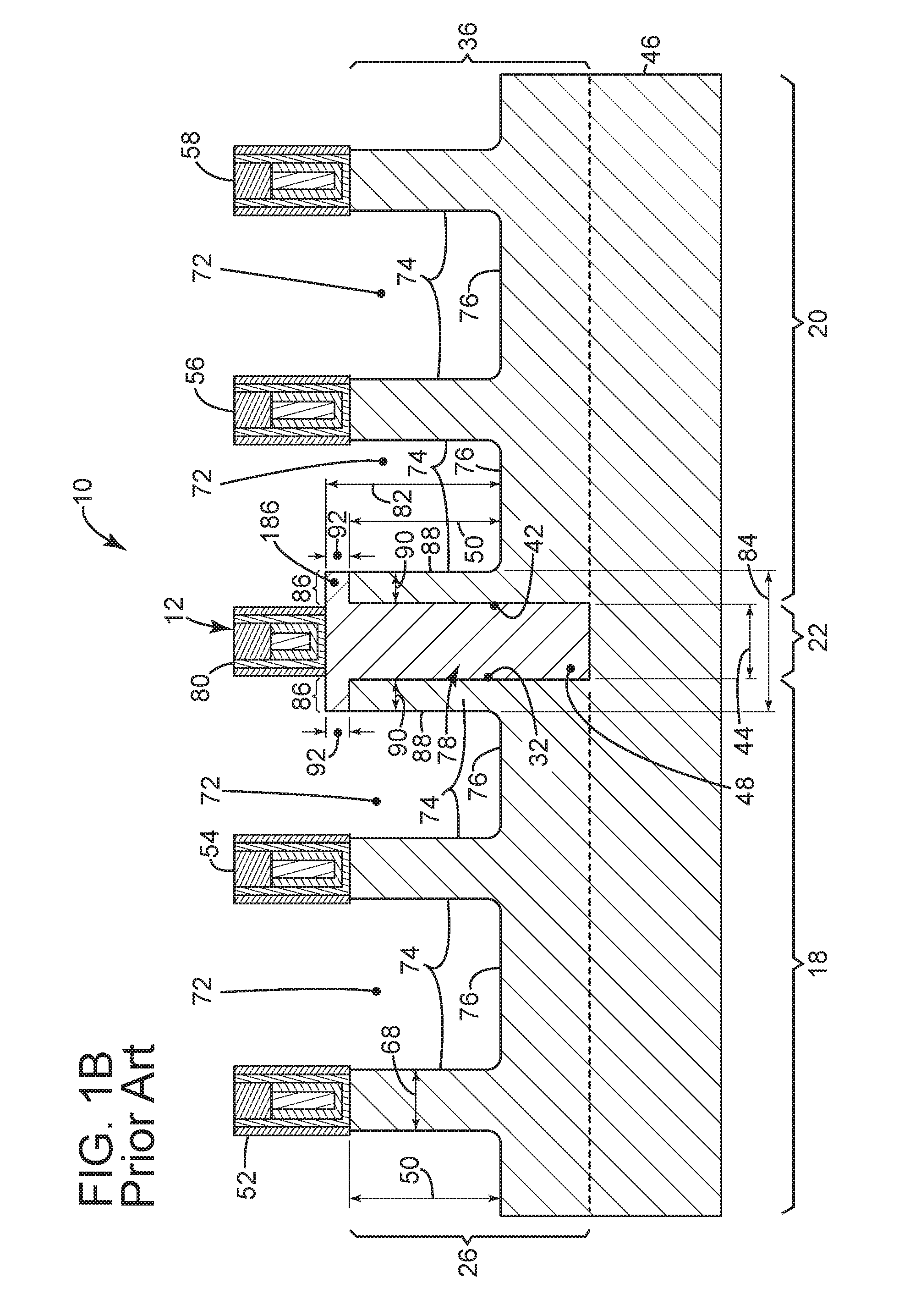
[0062]Referring to FIGS. 1A, 1B and 1C, an exemplary embodiment of a structure 10 for an integrated circuit formed utilizing FinFET technology and having a prior art single diffusi...


PUM


Abstract

A method of forming a single diffusion break includes etching rows of fins into a substrate of a structure from a patterned fin hardmask, the remaining fin hardmask being self-aligned with the fins. A first dielectric fill material is disposed and planarized over the structure to expose the fin hardmask. A photoresist layer is disposed over the structure. An isolation region is patterned across the fins to form first and second parallel fin arrays, wherein any remaining photoresist layer has self-aligned edges which are self-aligned with the isolation region. The self-aligned edges are trimmed to expose end portions of the fin hardmask. The exposed end portions are removed. The remaining photoresist layer is removed. A second dielectric fill material is disposed and planarized over the structure to form a base for a single diffusion break (SDB) in the isolation region.

Description

TECHNICAL FIELD[0001]The present invention relates to semiconductor devices and methods of fabricating the same. More specifically, the invention relates to single diffusion break structures and methods of making the same.BACKGROUND[0002]With constant down-scaling and increasingly demanding requirements to the speed and functionality of ultra-high density integrated circuits, semiconductor devices, such as transistors, diodes, capacitors and the like, need to continuously reduce space between active (Rx) regions on a semiconductor substrate. More specifically, as integrated circuits are scaled down, the shallow trench isolation (STI) regions used to electrically isolate Rx regions must also be scaled down.[0003]Conventionally, multiple Rx regions in a semiconductor integrated circuit typically include arrays of parallel extending fins having distal ends abutting the edges of each Rx region. By way of example, this is particularly the case for FinFET technology at the 14 nm node and ...

Claims


Application Information

Patent Timeline
IPC IPC(8): H01L27/088H01L29/66H01L21/3105H01L21/027H01L21/311H01L21/8234H01L29/06H01L21/308
CPCH01L27/0886H01L21/823431H01L21/308H01L21/31051H01L21/0273H01L21/823481H01L21/31111H01L29/66545H01L21/823437H01L29/0649
Inventor ZANG, HUICIAVATTI, JEROMECHI, MIN-HWA
Owner GLOBALFOUNDRIES INC
Why Eureka
Try Eureka