Chemical vapor deposition apparatus and method of forming thin layer using same

Inactive Publication Date: 2005-02-03
SAMSUNG ELECTRONICS CO LTD
View PDF2 Cites 8 Cited by
  • Summary
  • Abstract
  • Description
  • Claims
  • Application Information

AI Technical Summary

Benefits of technology

[0008] To solve the above and other problems, the present invention provides, among other things, a chemical vapor deposition (CVD) apparatus and a method of forming a thin layer which capable of improving poor thickne

Problems solved by technology

As a circuit line width decreases, technical limitations occur when using conventional technology when depositing wires formed of a material such as Al in the manufacturing of a semiconductor device.
Thus, a physical vapor deposition (PVD) method, such as sputtering, is not effectively employed.
In particular, as an aperture of a wafer becomes large and a device is scal

Method used


Image

  • Chemical vapor deposition apparatus and method of forming thin layer using same
  • Chemical vapor deposition apparatus and method of forming thin layer using same
  • Chemical vapor deposition apparatus and method of forming thin layer using same

Examples


Embodiment Construction

[0025] The present invention will now be described more fully with reference to the accompanying drawings in which exemplary embodiments of the invention are shown.

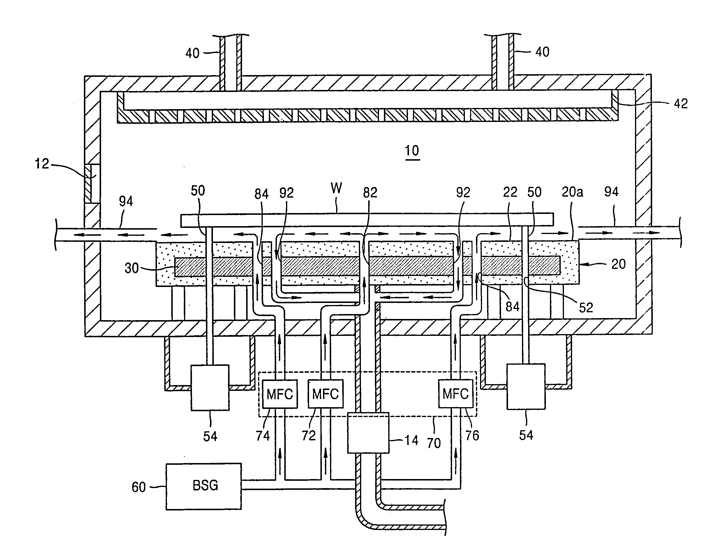
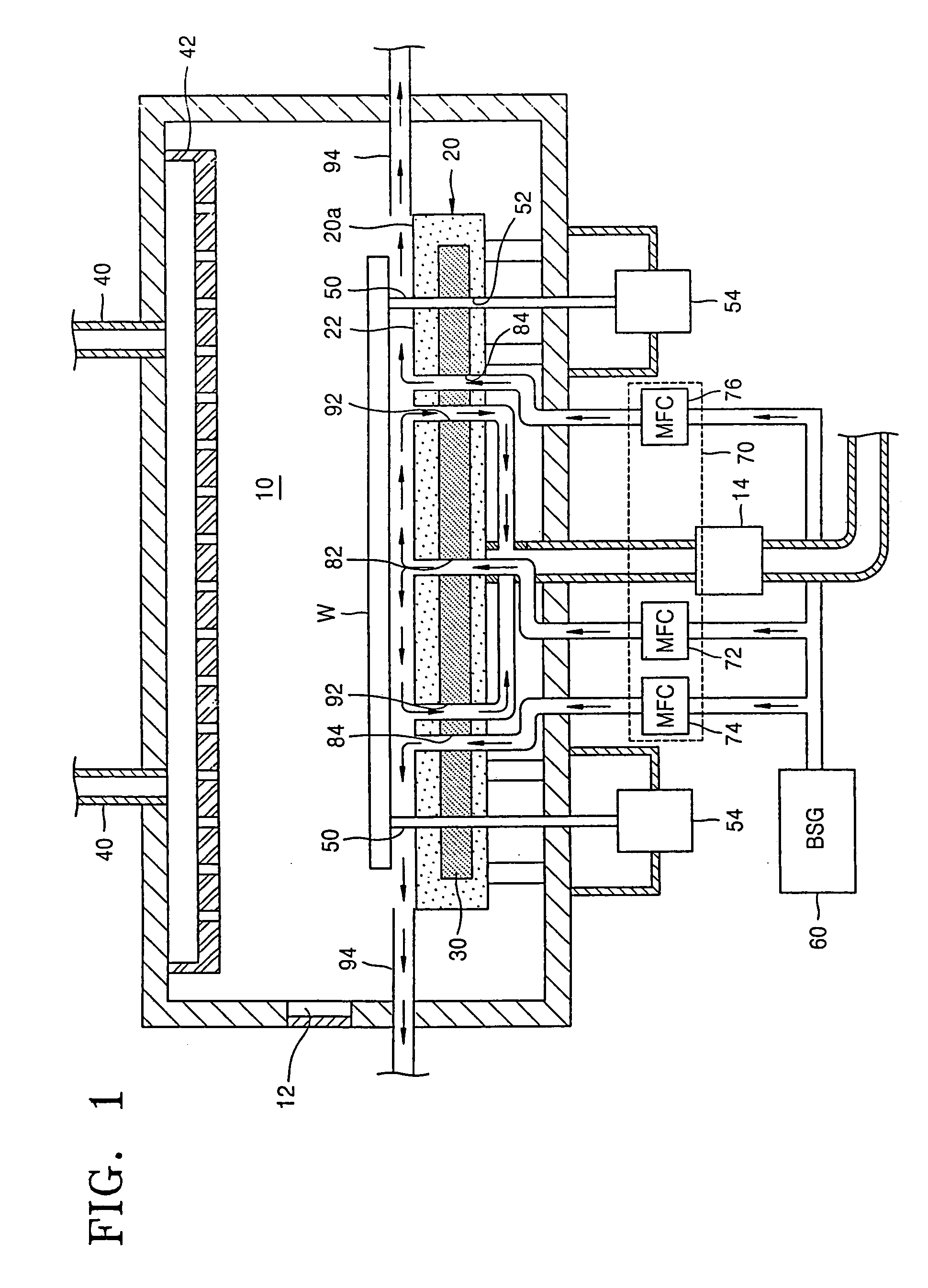
[0026] Referring to FIG. 1, a CVD apparatus comprises a reaction chamber 10 with an entrance 12 which allows a robotic arm (not shown) to enter so that a wafer W can be loaded into or unloaded from the reaction chamber 10. The reaction chamber 10 is maintained under a vacuum using a vacuum pump 14. Here, for instance, the reaction chamber 10 is an Al deposition chamber so as to form an Al layer on the wafer W. When a Ti or TiN layer is exposed on the wafer W, the CVD apparatus, which will be explained below, will operate more effectively.

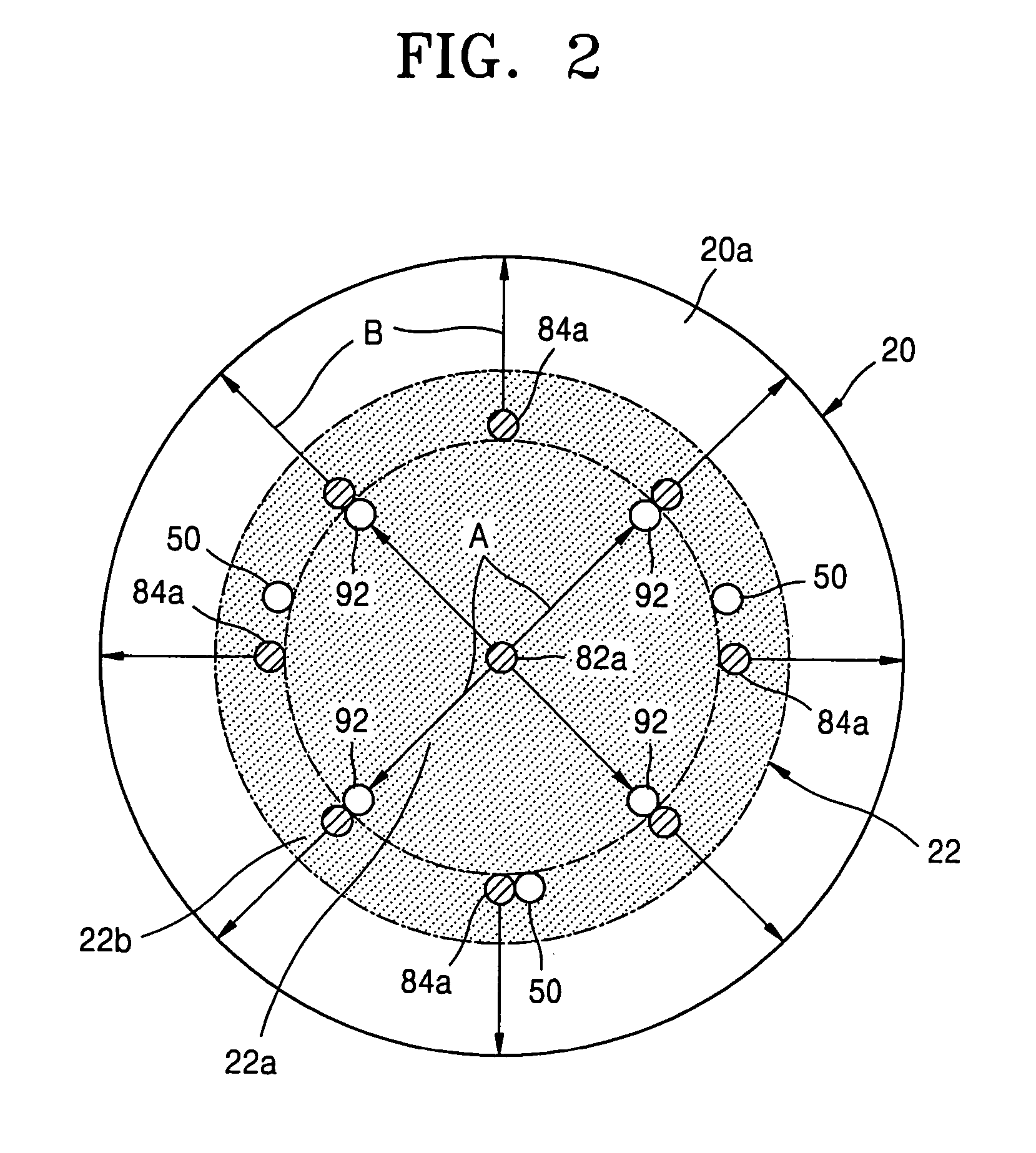
[0027] A heater table 20 is located in the reaction chamber 10. The heater table 20 has an upper surface 20a that includes a wafer supporting area 22, over which the wafer W is maintained. The heater table 20 includes a heater 30 which heats the wafer supporting area 22 to a required ma...


PUM

PropertyMeasurementUnit
Temperatureaaaaaaaaaa
Flow rateaaaaaaaaaa
Areaaaaaaaaaaa

Abstract

In one embodiment, a chemical vapor deposition (CVD) apparatus comprising a plurality of backside gas (BSG) passages that pass through a heater table that controls a temperature of a plurality of local areas on a wafer and a method of forming a thin layer using the CVD apparatus are provided. The heater table comprises a wafer supporting area divided into a plurality of local areas that correspond to the local areas of the wafer. Each of the BSG passages has a BSG outlet that supplies the BSG, heated by a heater, to the local areas. Flow controllers control the flow through each of the BSG passages, thereby controlling the temperature of local areas.

Description

BACKGROUND OF THE INVENTION [0001] This application claims the priority of Korean Patent Application No. 2003-53396, filed on Aug. 1, 2003, in the Korean Intellectual Property Office, the disclosure of which is incorporated herein in its entirety by reference. [0002] 1. Field of the Invention [0003] The present invention relates to an apparatus for manufacturing a semiconductor device and a method of forming a thin layer of a semiconductor device using the apparatus, and more particularly, to a chemical vapor deposition (CVD) apparatus and a method of forming a thin layer on a wafer using the apparatus. [0004] 2. Description of the Related Art [0005] As a circuit line width decreases, technical limitations occur when using conventional technology when depositing wires formed of a material such as Al in the manufacturing of a semiconductor device. Therefore, a technique of filling a contact hole as a connection portion of lower conductive layer and an upper Al wires or a via hole a c...

Claims


Application Information

Patent Timeline
IPC IPC(8): H01L21/205C23C16/00C23C16/02C23C16/06C23C16/458C23C16/46H01L21/285H01L21/3205
CPCC23C16/0272C23C16/06C23C16/4586H01L21/32051C23C16/466H01L21/28556C23C16/46H01L21/205
Inventor SEO, JUNG-HUNPARK, YOUNG-WOOKHAN, JAE-JONG
Owner SAMSUNG ELECTRONICS CO LTD
Why Eureka
Try Eureka