Method for manufacturing twin bit structure cell with Al2O3/nano-crystalline Si layer

a technology of nano-crystalline si layer and twin bit structure, which is applied in the field of integrated circuits, can solve the problems of high cost of integrated circuit or chip fabrication facilities, difficult devices, and limited process use of integrated fabrication processes, and achieve the effect of cost-effective implementation

Active Publication Date: 2012-02-14
SEMICON MFG INT (SHANGHAI) CORP +1
View PDF17 Cites 8 Cited by
  • Summary
  • Abstract
  • Description
  • Claims
  • Application Information

AI Technical Summary

Benefits of technology

[0009]Many benefits are achieved by ways of the present invention over conventional techniques. For example, embodiments according to the present invention provide a method to form a reliable twin bit cell structure. According to a specific embodiment, a gate structure is formed on top of a dielectric layer, which is later selectively etched to form undercut regions. The undercut regions are used to accommodative conductive materials such as aluminum oxide material. For example, the conductive material is used to hold charges to stores bits. It is to be appreciated that because of the innovation afforded by the present invention to provide undercut regions, various etching processes according to the present invention are self-aligned. Among other things, the technique according to the present invention for forming twin-bit device allows further scaling down of the device in comparison of convention techniques. Furthermore, various processes and techniques can be compatible with conventional systems and equipments, thereby allow cost effective implementation. There are other benefits as well.

Problems solved by technology

An integrated circuit or chip fabrication facility can cost hundreds of millions, or even billions, of U.S. dollars.
Making devices smaller is very challenging, as each process used in integrated fabrication has a limit.
An example of such limitation lies in manufacture of memory devices.
As feature size continues to shrink, a twin bit cell structure becomes difficult to apply as it is difficult to control the gates independently.
One of the challenges in semiconductor has been the processing of manufacturing twin-bit cell structure for non-volatile memory devices, such as popular flash based memory devices.
Among other things, the conventional system and method for manufacturing cells with twin-bit structures are limited when it is required to scaling down the cell size.

Method used


Image

  • Method for manufacturing twin bit structure cell with Al2O3/nano-crystalline Si layer
  • Method for manufacturing twin bit structure cell with Al2O3/nano-crystalline Si layer
  • Method for manufacturing twin bit structure cell with Al2O3/nano-crystalline Si layer

Examples


Embodiment Construction

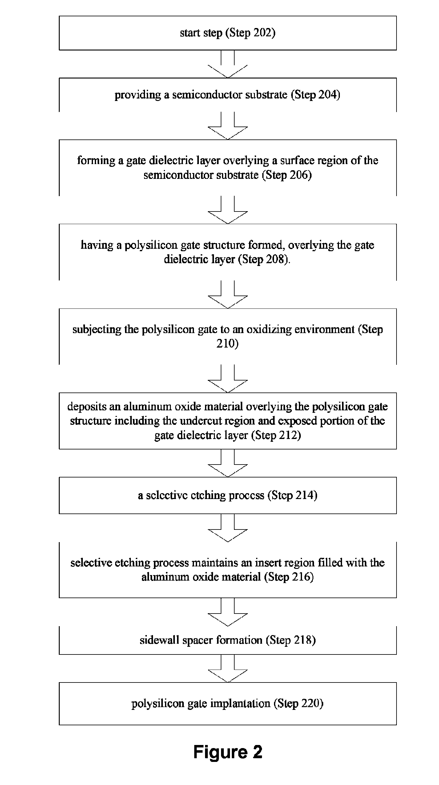
[0015]According to embodiments of the present invention, techniques directed to manufacturing memory devices are provided. Merely by ways of example, embodiments according to the present invention provide a method and a structure for manufacturing a twin bit cell structure for a non-volatile memory device. But embodiments according to the present invention can be applied to manufacturing of other devices.

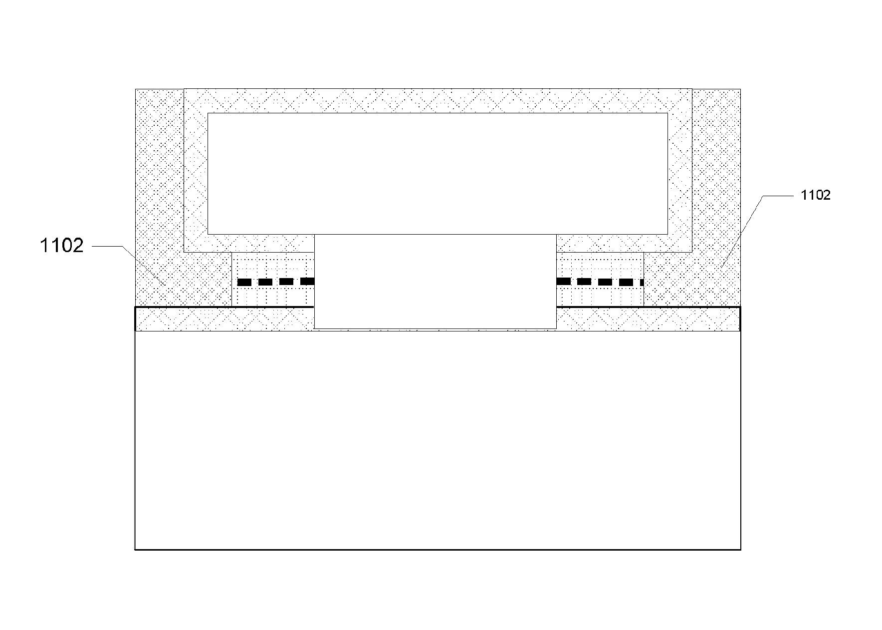
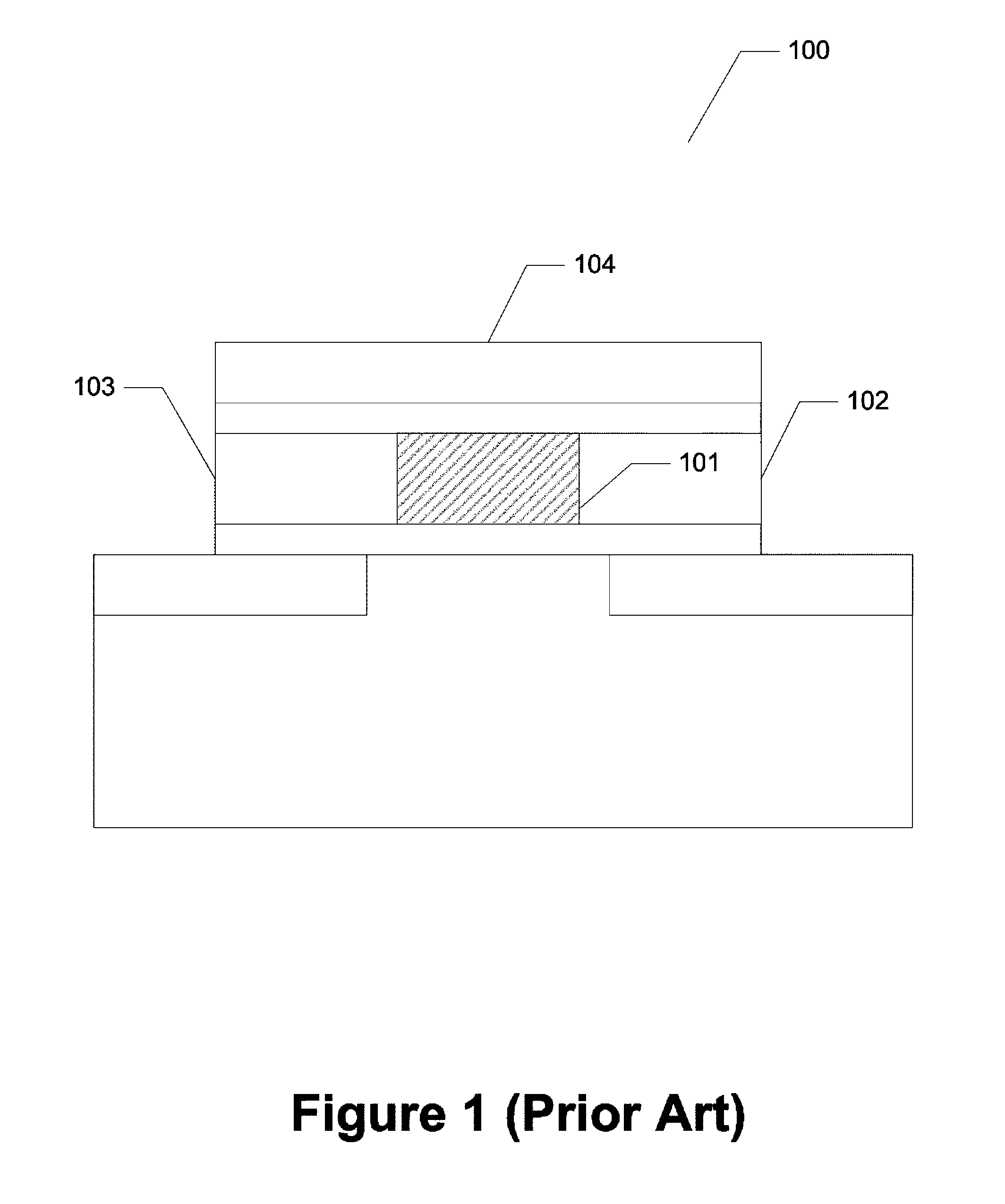
[0016]FIG. 1 is a simplified twin bit cell structure using a conventional method for fabrication. As shown in FIG. 1, the twin-bit structure 100 has two conductive regions 102 and 103 that can be configured to hold charges. The two conductive regions are separated by an isolation region 101. A control gate 104 overlays the conductive regions.

[0017]As an example, the twin bit cell structure shown in FIG. 1 is manufactured using the following steps:[0018]1. provide a p-type substrate;[0019]2. form a gate oxide layer overlaying the substrate;[0020]3. perform low-pressure chemical vapor...


PUM


Abstract

A method and system for forming a non-volatile memory structure. The method includes providing a semiconductor substrate and forming a gate dielectric layer overlying a surface region of the semiconductor substrate. A polysilicon gate structure is formed overlying the gate dielectric layer. The method subjects the polysilicon gate structure to an oxidizing environment to cause formation of a first silicon oxide layer overlying the polysilicon gate structure and formation of an undercut region underneath the polysilicon gate structure. An aluminum oxide material is formed overlying the polysilicon gate structure filling the undercut region. In a specific embodiment, the aluminum oxide material has a nanocrystalline silicon material sandwiched between a first aluminum oxide layer and a second aluminum oxide layer. The aluminum oxide material is subjected to a selective etching process while maintaining the aluminum oxide material in an insert region in a portion of the undercut region. The method forms a sidewall structure overlying a side region of the polysilicon gate structure.

Description

CROSS-REFERENCES TO RELATED APPLICATIONS[0001]This application claims priority to Chinese Application No. 200910056728.5 filed on Aug. 20, 2009 commonly assigned and is hereby incorporated by reference for all purposes. This application is also related to the following co-pending U.S. patent applications, all of which are commonly owned and are hereby incorporated by reference for all purpose: U.S. patent application Ser. No. 12 / 978,346, filed Dec. 23, 2010, U.S. patent application Ser. No. 12 / 978,473, filed Dec. 24, 2010, U.S. patent application Ser. No. 12 / 965,808, filed Dec. 10, 2010, U.S. patent application Ser. No. 12 / 968,264, filed Dec. 14, 2010, and U.S. patent application Ser. No. 12 / 969,563, filed Dec. 15, 2010.BACKGROUND OF THE INVENTION[0002]The present invention is directed to integrated circuits and their processing for the manufacture of semiconductor devices. More particularly, the invention provides a method and a device for forming a twin bit cell structure for semi...

Claims


Application Information

Patent Timeline
Patent Type & Authority Patents(United States)
IPC IPC(8): H01L21/336H01L21/461H01L21/8242
CPCB82Y10/00H01L21/28273H01L29/42332H01L29/7887H01L29/40114
Inventor FUMITAKE, MIENO
Owner SEMICON MFG INT (SHANGHAI) CORP
Why Eureka
Try Eureka