
Semiconductor device and semiconductor device manufacturing method

a semiconductor device and manufacturing method technology, applied in the direction of semiconductor devices, basic electric elements, electrical appliances, etc., can solve the problems of dielectric breakdown at the finger portion f, insufficient relaxation, etc., and achieve the effect of reducing the resistance to voltag

Active Publication Date: 2017-01-24
LAPIS SEMICON CO LTD
View PDF2 Cites 0 Cited by
  • Summary
  • Abstract
  • Description
  • Claims
  • Application Information

AI Technical Summary

Benefits of technology

[0026]According to the present invention, a semiconductor device in which decreases in withstand voltage are suppressed, and a manufacturing method for the semiconductor device can be provided.

Problems solved by technology

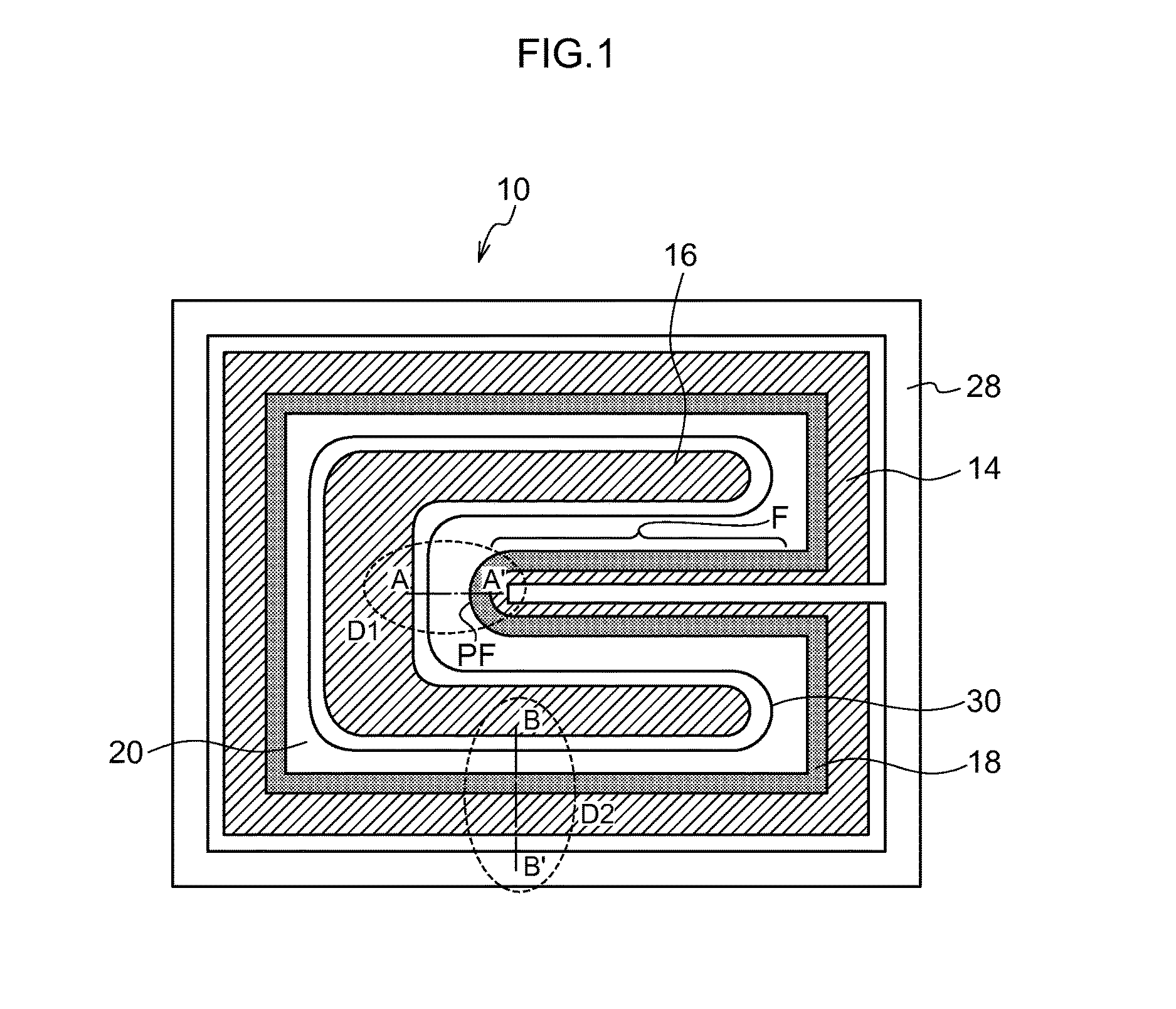
Field relaxation is therefore insufficient in the vicinity of the finger portion F, and in particular, in the vicinity of the leading end PF of the finger portion F, and there is an issue in that dielectric breakdown is liable to occur at the finger portion F, and in particular, at the leading end PF when high voltage is applied to the drain layer or the source layer.

Method used


Image

  • Semiconductor device and semiconductor device manufacturing method
  • Semiconductor device and semiconductor device manufacturing method
  • Semiconductor device and semiconductor device manufacturing method

Examples


Embodiment Construction

[0035]Explanation follows regarding a semiconductor device of an exemplary embodiment, and a manufacturing method for the semiconductor device, with reference to FIG. 1 to FIG. 4F. The present exemplary embodiment explains an example of a mode in which the semiconductor device according to the present invention is applied to an N-type metal oxide semiconductor field effect transistor (MOSFET; also sometimes referred to as a MOS transistor below).

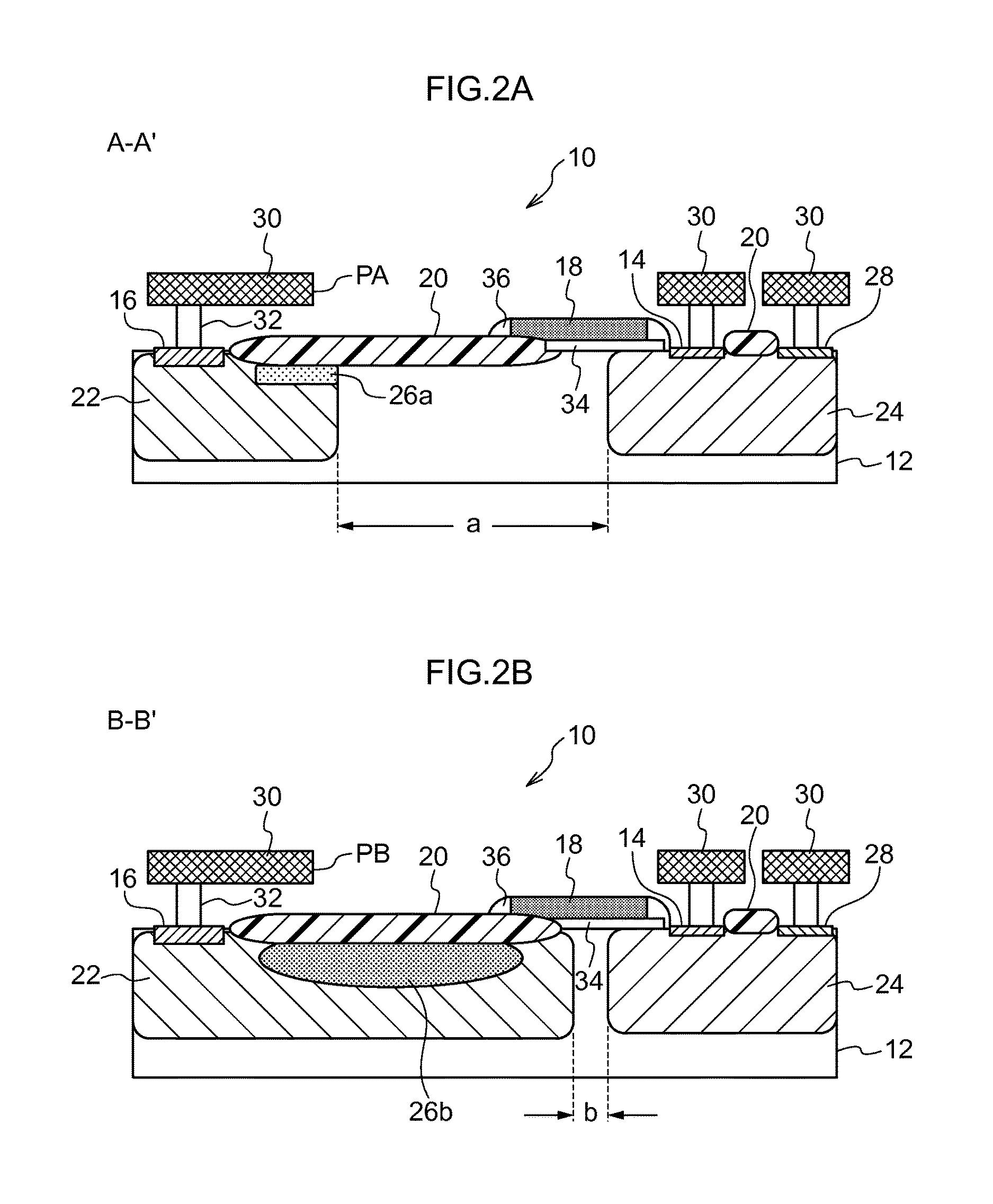
[0036]FIG. 1 is a plan view of a MOS transistor 10 according to the present exemplary embodiment. FIG. 2A is a cross-section taken along line A-A′ in FIG. 1. FIG. 2B is a cross-section taken along line B-B′ in FIG. 1. As illustrated in FIG. 1, a region in the vicinity of cross-section A-A′ is also referred to as region D1, and a region in the vicinity of the cross-section B-B′ is also referred to as region D2 hereafter.

[0037]As illustrated in FIG. 1, the MOS transistor 10 according to the present exemplary embodiment is configured including ...


PUM


Abstract

A semiconductor device includes a semiconductor substrate; a first semiconductor region that includes an extension portion extending in a specific direction at a specific width as viewed along a direction orthogonal to the main surface; a second semiconductor region that is shaped to include a portion running along the extension portion of the first semiconductor region as viewed along the direction orthogonal to the main surface; a field relaxation layer that relaxes a field generated between the first semiconductor region and the second semiconductor region, that is formed on the second semiconductor region side of the main surface, and that is formed by a semiconductor layer; and a conductor that is connected to the second semiconductor region, and that has an end portion on the first conductor region side positioned within the range of the field relaxation layer.

Description

CROSS-REFERENCE TO RELATED APPLICATION[0001]This application is based on and claims priority under 35 USC 119 from Japanese Patent Application No. 2014-166508 filed on Aug. 19, 2014, the disclosure of which is incorporated by reference herein.BACKGROUND[0002]Technical Field[0003]The present invention relates to a semiconductor device and a manufacturing method for the semiconductor device.[0004]Related Art[0005]Attention is being given to various approaches for maintaining a high withstand voltage in semiconductors for high power applications. For example, a field effect transistor described by Japanese Patent Application Laid-Open (JP-A) No. H05-259454 is known as a semiconductor device for high withstand voltage applications according to conventional technology.[0006]A field effect transistor 50 described by JP-A No. H05-259454 is illustrated in FIG. 5, FIG. 6A, and FIG. 6B. FIG. 5 is a plan view of the field effect transistor 50, FIG. 6A is a cross-section of the field effect tra...

Claims


Application Information

Patent Timeline
Patent Type & Authority Patents(United States)
IPC IPC(8): H01L29/00H01L29/66H01L29/78H01L29/06H01L29/10
CPCH01L29/0696H01L29/063H01L29/66659H01L29/7835H01L29/0653H01L29/1045H01L29/0615H01L29/66477H01L29/78
Inventor MORI, TORU
Owner LAPIS SEMICON CO LTD
Learn More