Optical lattice clock, clock device and laser light source

a technology of optical lattice clock and laser light source, which is applied in the direction of laser details, pulse automatic control, active medium shape and construction, etc., can solve the problems of difficult to obtain portability in such optical atomic clocks, and achieve the effect of miniaturizing optical lattice clocks and high precision

Active Publication Date: 2017-01-24
RIKEN
View PDF4 Cites 6 Cited by
  • Summary
  • Abstract
  • Description
  • Claims
  • Application Information

AI Technical Summary

Benefits of technology

[0010]In contrast, the problem of interaction between the atoms and the wall of the container or the like mentioned above is substantially solved by the optical lattice clocks. Moreover it is possible to improve preciseness in accordance with the operational principle, particularly when a special wavelength called a magic wavelength for the optical lattice is adopted. On top or that, increasing the number of atoms engaged in clock transitions in general, or, to be more specific, increasing substantial volume of a spatial region where the atoms can be trapped in the optical lattice, would be most favorable in improving accuracy for increasing the number of trapped atoms.
[0011]The present disclosure contributes to realization of an optical lattice clock, a clock device, and a laser light source, of high precision, by providing specified structures that make it possible to increase the number of atoms, while taking advantage of substantially zero interaction between atoms engaged in clock transitions and wall of container or the like.Solution to Problem
[0023]According to any aspect of the present disclosure, operation of high precision is achieved, and it is possible to miniaturize optical lattice clocks.

Problems solved by technology

However, it is not easy to obtain portability in such optical atomic clocks because they are equipped with ultra-stable laser light sources that use bulky vacuum facility equipment and anti-vibration devices of high precision.

Method used


Image

  • Optical lattice clock, clock device and laser light source
  • Optical lattice clock, clock device and laser light source
  • Optical lattice clock, clock device and laser light source

Examples


Embodiment Construction

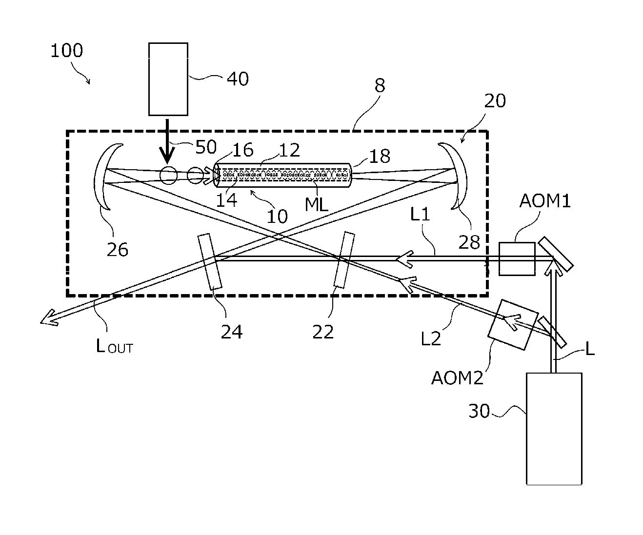
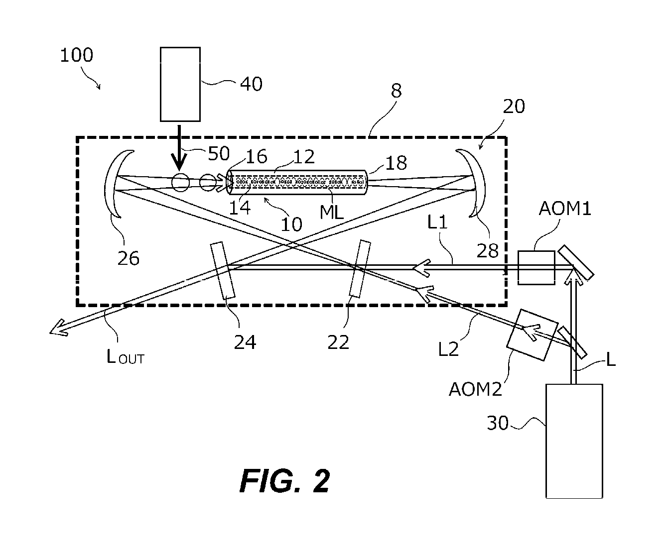
[0030]The embodiments of optical lattice clocks of the present disclosure will be described based on the drawings. For all drawings, common reference numerals are given to common part or element unless otherwise noted.

[0031]1. Principle of Conventional Optical Lattice Clock

[0032]In order to explain operation principles governing optical lattice clocks in the present embodiment, described in the first place is operation and accuracy improvement in the conventional atomic clocks (1-2). Then conventional optical lattice clocks are described (1-3).

[0033]1-2. Operation of Conventional Atomic Clocks

[0034]To begin with, conventional atomic clocks that utilize transition frequency of clock transitions of atoms are introduced while paying attention to dominant factors on their accuracy as well as approaches concerning the factors. Accuracy in atomic clocks, or uncertainty of clock operation, is determined by, in short, how exactly transition frequency is measured for the clock transitions, a...


PUM


Abstract

Various embodiments improve accuracy by increasing the number of atoms engaged in a clock transitions in an optical lattice clock. An exemplary optical lattice clock an embodiment comprises an optical waveguide, an optical path, a laser light source, and a laser cooler. The optical path has a hollow pathway that extends from a first end to a second end while being surrounded with a tubular wall, which is used as a waveguide path. The optical path passes between mirrors and through the pathway. The laser light source supplies to the optical path a pair of lattice lasers (L1 and L2) propagating in opposite directions with each other. The laser cooler supplies cooled atoms that have two levels of electronic states associated with a clock transition to the vicinity of the first end of the optical waveguide.

Description

TECHNICAL FIELD[0001]The present disclosure is related to an optical lattice clock, a clock device, and a laser light source. More specifically, the present disclosure is related to an optical lattice clock, a clock device, and a laser light source, each of which uses principle of optical lattice clocks for high precision operation.BACKGROUND ART[0002]Atomic clocks have been conventionally used for a reference time standard. The atomic clocks have been generally accepted as representative ones of high precision clocks and have been adopted for primary references of time as an example. On top of that, the atomic clocks have been applied to fields that require high preciseness such as GPS (Global Positioning System), where each GPS satellite is equipped with an atomic clock. Generally speaking, atomic clocks utilize electromagnetic waves in a microwave region for a frequency reference, which waves are produced through transitions between electronic levels (hereinafter called “clock tr...

Claims


Application Information

Patent Timeline
Patent Type & Authority Patents(United States)
IPC IPC(8): H03L7/26H01S3/067G04F5/14
CPCH03L7/26G04F5/14H01S3/06791
Inventor KATORI, HIDETOSHI
Owner RIKEN
Why Eureka
Try Eureka