Display device

a display device and display technology, applied in semiconductor devices, semiconductor/solid-state device details, electrical devices, etc., can solve the problems of difficult to display an accurate image corresponding to a video signal, signal delay caused, etc., to achieve the effect of avoiding unnecessary parasite capacitance, reducing parasite capacitance size, and ensuring the easiness of manufacturing a display device having such a wiring

Active Publication Date: 2017-03-07
SONY CORP
View PDF19 Cites 3 Cited by
  • Summary
  • Abstract
  • Description
  • Claims
  • Application Information

AI Technical Summary

Benefits of technology

The patent text describes a display device with improved image display performance that is achieved through a simple configuration. The device includes an insulating layer with a recess or projection that separates electrode layers and reduces unnecessary parasite capacitance between the electrodes. The wiring in the drive circuit is placed in the overlap region of the insulating layer and the recess or projection in the insulating layer, which prevents the formation of unnecessary parasite capacitance and improves image display performance. Additionally, the device includes a gap region between neighboring light emitting elements, where the insulating layer has the recess or projection, which further reduces parasite capacitance and improves image display performance. Overall, this display device design ensures accurate image display and suppresses unintended signal delay.

Problems solved by technology

Since the signal line Z120A is a path for supplying voltage of a video signal according to luminance information from an external signal supply source, even the unnecessary parasite capacitance Cz is formed, signal delay is caused.
In some cases, it is difficult to display an accurate image corresponding to a video signal.
However, it disturbs compactification of the entire organic EL display, so that it is unrealistic.

Method used


Image

  • Display device
  • Display device
  • Display device

Examples


Embodiment Construction

[0026]Embodiments of the present application will be described below in detail with reference to the drawings.

[0027]Modes for carrying out the present application (hereinbelow, called embodiments) will be described in detail below with reference to the drawings.

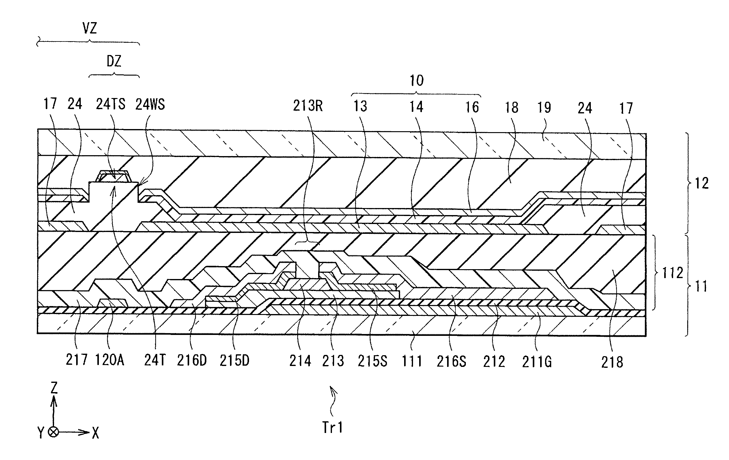
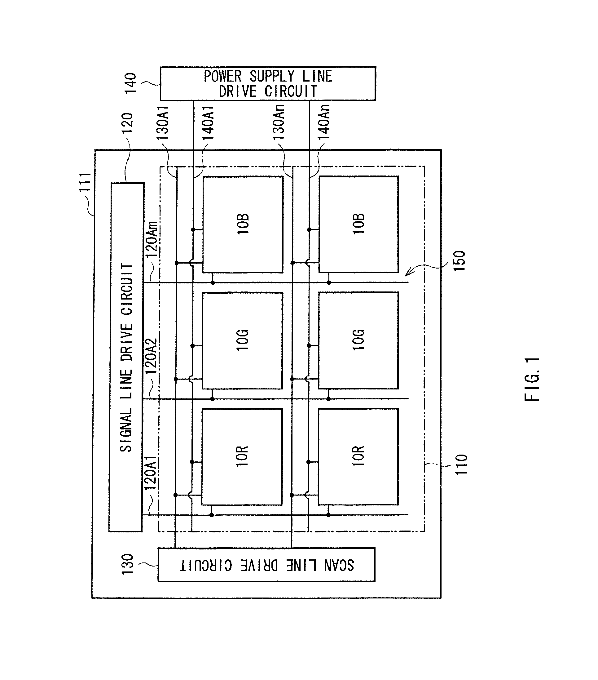
[0028]FIG. 1 illustrates the configuration of a display device using an organic light emitting element according to an embodiment. A display device is used as an organic light emitting color display device of a very thin type or the like. In the display device, a display region 110 is formed on a substrate 111. In the periphery of the display region 110 on the substrate 111, for example, a signal line drive circuit 120, a scan line drive circuit 130, and a power supply line drive circuit 140 as drivers for displaying video images are formed.

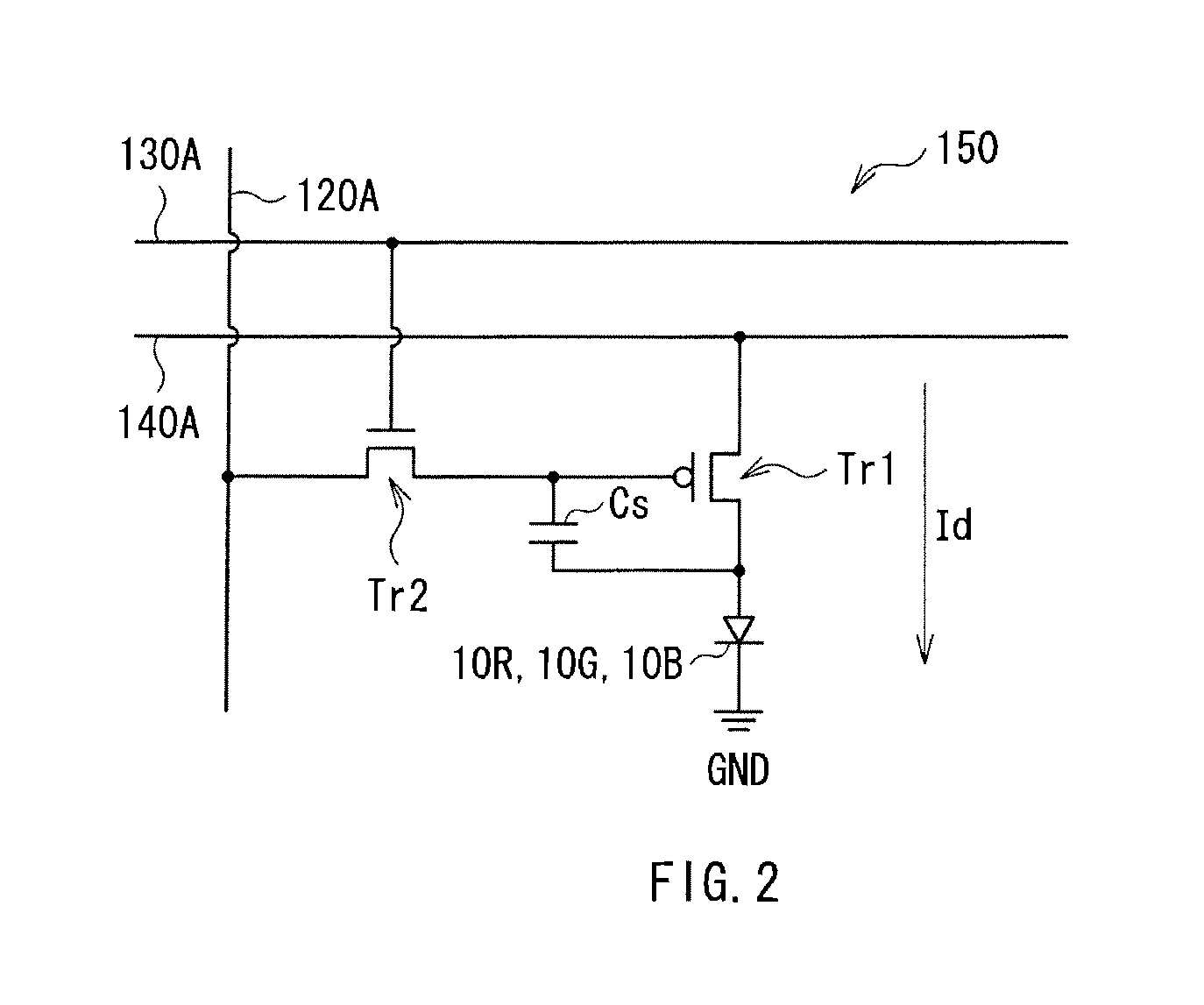
[0029]In the display region 110, a plurality of organic light emitting elements 10 (10R, 10G, and 10B) disposed two-dimensionally in a matrix and a pixel drive circuit 150 for driving the ...


PUM


Abstract

A display device includes, on a substrate, light emitting elements each formed by sequentially stacking a first electrode layer, an organic layer including a light emission layer, and a second electrode layer and arranged in first and second directions which cross each other, a drive circuit including drive elements that drive light emitting elements, and a wiring extending in the first direction, and an insulating layer disposed in a gap region sandwiched by the light emitting elements neighboring in the second direction and having a recess or a projection. The wiring is disposed in an overlap region overlapping with the recess or the projection in the insulating layer in a thickness direction, in the gap region, and the second electrode layers in the light emitting elements neighboring in the second direction are separated from each other by the recess or the projection in the insulating layer.

Description

CROSS REFERENCES TO RELATED APPLICATIONS[0001]The present application is a continuation of U.S. patent application Ser. No. 14 / 512,028, filed on Oct. 10, 2014, which application is a continuation of U.S. patent application Ser. No. 13 / 782,130, filed on Mar. 1, 2013, and issued as U.S. Pat. No. 8,866,133 on Oct. 21, 2014, which application is a continuation of U.S. patent application Ser. No. 13 / 159,577 filed on Jun. 14, 2011 and issued as U.S. Pat. No. 8,399,892 on Mar. 19, 2013, which claims priority to Japanese Priority Patent Application JP 2010-147859 filed in the Japan Patent Office on Jun. 29, 2010, the entire content of which is hereby incorporated by reference.BACKGROUND[0002]The present application relates to a display device having a light emitting element of a self-emitting type including an organic layer.[0003]In recent years, as a display device replacing a liquid crystal display, an organic EL display using an organic light emitting element of a self-emitting type incl...

Claims


Application Information

Patent Timeline
Patent Type & Authority Patents(United States)
IPC IPC(8): H01L27/32H01L51/52H01L23/50H01L27/12H10K99/00
CPCH01L27/3276H01L23/50H01L27/32H01L27/3246H01L27/3258H01L27/3262H01L51/5203H01L51/5228H01L27/124H01L27/1248H01L2924/0002H01L2924/00H10K59/122H10K59/131H10K50/805H10K50/824H10K59/00H10K59/124H10K59/1213H10K59/1201
Inventor SAGAWA, HIROSHI
Owner SONY CORP
Why Eureka
Try Eureka