
Method for bonding metallic contact areas with solution of a sacrificial layer applied on one of the contact areas

a technology of contact area and solution, applied in the direction of semiconductor/solid-state device testing/measurement, semiconductor device details, semiconductor/solid-state device testing/measurement, etc., can solve the problem of not being able to make optimal contact between unpolished solid surfaces and substrates at correspondingly high roughness, and using very high temperatures and pressures

Active Publication Date: 2017-05-02
EV GRP E THALLNER GMBH
View PDF37 Cites 7 Cited by
  • Summary
  • Abstract
  • Description
  • Claims
  • Application Information

AI Technical Summary

Benefits of technology

[0026]It is advantageous if the sacrificial layer, especially Si, is applied in-situ jointly with the bond layer, especially Cu, onto the substrate. This prevents the formation of oxide on the bond layer.
[0055]In special embodiments the water is introduced by a bubbler into the reaction chamber in which the substrate is located. To do this, inert gases such as for example argon, helium, and nitrogen are driven through a water bath. The inert gas supports the water during evaporation and saturates the reaction chamber with water vapor. The water condenses on the surface of the substrate and forms a very thin water film. Cooling the substrate can support the condensation of the water.
[0060]A version of the sacrificial layer which is very thin enables a rapid diffusion of atoms of the sacrificial layer, especially solely, into the bond regions. The diffusion is accelerated and / or promoted by heat treatment. Preferably the atoms of the sacrificial layer dissolve completely in the material of the bond region and / or of the bulk material. A process is also conceivable in which the atoms of the bond regions dissolve in the sacrificial layer; viewed technically, this is identical to the above described version due to the extremely small thickness of the sacrificial layer.

Problems solved by technology

In most cases this joining takes place permanently, therefore irreversibly, which means that the separation of the two substrates after the bonding process is no longer possible without their destruction or at least their partial destruction.
Unpolished solid surfaces however do not make optimum contact at correspondingly high roughness.
The disadvantage in these metal bonds therefore consists mainly in the use of very high temperatures and pressures to ensure a joining of the two substrates at all.
In any case this oxide layer is in turn unwanted if the intention is to bond two metals directly to one another, for example to join two conductive contacts to one another.
Heat treatment of the substrates dictates correspondingly long heat-up and cooling times. The high temperatures can moreover lead to disruptions in functional units such as for example microchips and mainly in memory chips and can damage them to the point of not being usable.

Method used


Image

  • Method for bonding metallic contact areas with solution of a sacrificial layer applied on one of the contact areas
  • Method for bonding metallic contact areas with solution of a sacrificial layer applied on one of the contact areas
  • Method for bonding metallic contact areas with solution of a sacrificial layer applied on one of the contact areas

Examples


Embodiment Construction

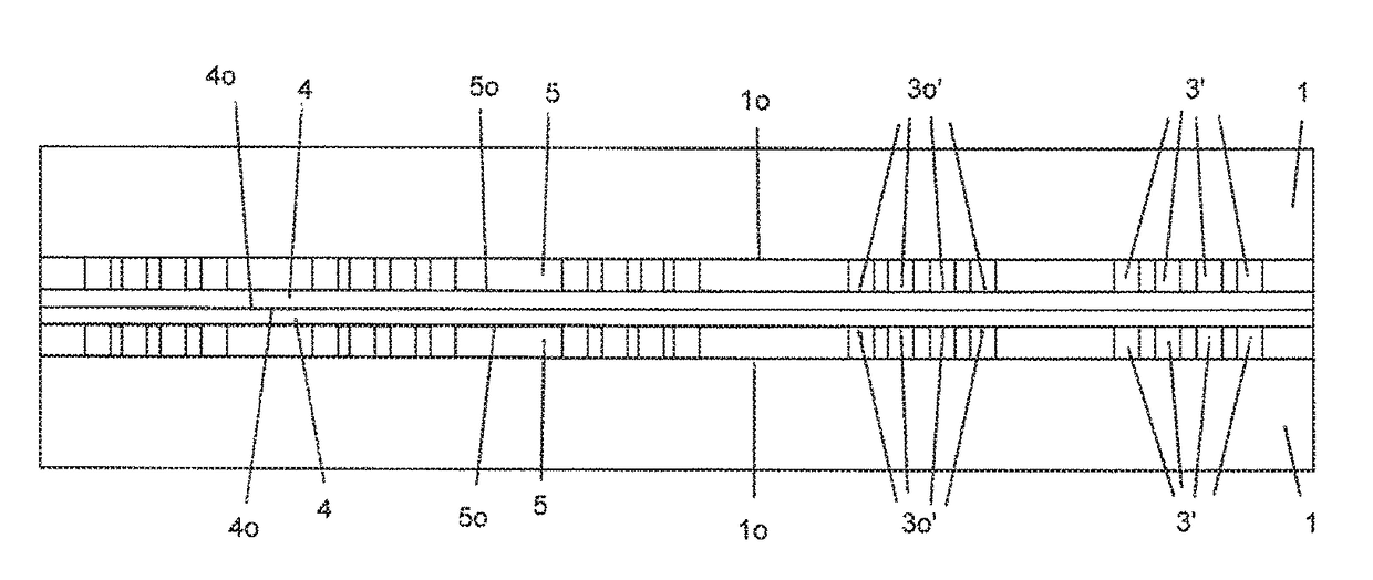
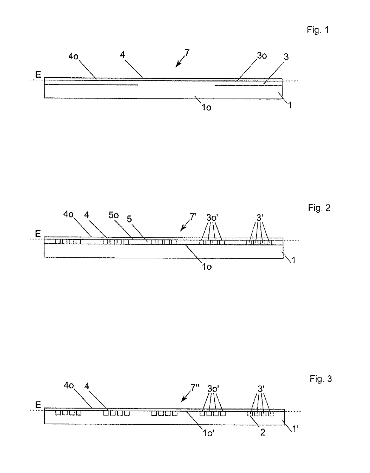
[0087]In the figures, the same components or components with the same effect are identified with the same reference numbers. The drawings show only schematically the embodiments of the invention and are not to scale. Thus mainly the relative thicknesses of the sacrificial layer, the bond regions and the substrates are disproportionate to one another, in exactly the same way as the ratio of the indicated thicknesses to the diameter of the substrates.

[0088]FIG. 1 shows a layer system 7 comprising a first substrate 1 with an interface 1o, a bond region 3 with a bond region surface 3o, and the sacrificial layer 4 with the sacrificial layer surface 4o. The bond region 3 extends in the first embodiment over the entire interface 1o of the substrate 1. The bond region surface 3o in this case forms a first contact surface of the first substrate 1. The bond region 3 can be in particular a material-integral (therefore comprising the same material) and / or monolithic component of the first subst...


PUM

PropertyMeasurementUnit
thicknessaaaaaaaaaa
thicknessaaaaaaaaaa
thicknessaaaaaaaaaa

Abstract

A method for bonding of a first, at least partially metallic contact surface of a first substrate to a second, at least partially metallic contact surface of a second substrate, with the following steps, especially the following progression: application of a sacrificial layer which is at least partially, especially predominantly soluble in the material of at least one of the contact surfaces to at least one of the contact surfaces, bonding of the contact surfaces with at least partial solution of the sacrificial layer in at least one of the contact surfaces.

Description

FIELD OF THE INVENTION[0001]This invention relates to a method for bonding of a first contact surface of a first substrate to a second contact surface of a second substrate.BACKGROUND OF THE INVENTION[0002]So-called boding technology has been used for several years in the semiconductor industry. Bonding technology allows joining of two or more substrates which are generally aligned very precisely to one another. In most cases this joining takes place permanently, therefore irreversibly, which means that the separation of the two substrates after the bonding process is no longer possible without their destruction or at least their partial destruction. When the substrates are joined it is shown that there are different chemical and physical mechanisms which cause a permanent connection. Nonmetallic surfaces are especially interesting. In nonmetallic surfaces the formation of a so-called prebond occurs by pure contact-making.[0003]This spontaneously forming, reversible connection of th...

Claims


Application Information

Patent Timeline
Patent Type & Authority Patents(United States)
IPC IPC(8): H01L21/00H01L23/00H01L21/66
CPCH01L24/83H01L24/03H01L24/05H01L24/06H01L24/27H01L24/29H01L24/32H01L24/743H01L2224/05647H01L2224/061H01L2224/274H01L2224/2741H01L2224/2745H01L2224/2781H01L2224/2784H01L2224/27444H01L2224/27452H01L2224/27464H01L2224/27845H01L2224/29023H01L2224/29028H01L2224/29187H01L2224/8301H01L2224/83011H01L2224/83012H01L2224/8312H01L2224/83013H01L22/12H01L2223/54426H01L2224/0345H01L2224/0381H01L2224/03452H01L2224/03602H01L2224/03616H01L2224/05561H01L2224/05564H01L2224/05567H01L2224/83026H01L2224/8383H01L2224/83121H01L2224/83203H01L2224/83907H01L2924/00014H01L2924/01029H01L2924/00012H01L2924/05442H01L2224/05552
Inventor REBHAN, BERNHARD
Owner EV GRP E THALLNER GMBH
Learn More