Vertical thin-channel memory

a thin-channel memory and vertical technology, applied in semiconductor devices, transistors, instruments, etc., can solve the problems of affecting the characteristics of read and program, the density of data storage can be limited, and the density of three-dimensional memory structure is limited, so as to improve the short channel performance, improve the performance, and short the effect of the channel length

Active Publication Date: 2017-07-04
MACRONIX INT CO LTD
View PDF41 Cites 42 Cited by
  • Summary
  • Abstract
  • Description
  • Claims
  • Application Information

AI Technical Summary

Benefits of technology

[0011]In an example described herein, the memory device comprises a plurality of stacks of conductive strips, the plurality of stacks including even stacks and odd stacks. A plurality of active pillars, arranged between corresponding even and odd stacks of conductive strips in the plurality of stacks, defines a multilayer array of interface regions at cross-points between opposing side surfaces of the active pillars and conductive strips in the corresponding even and odd stacks of conductive strips. The active pillars can include first and second vertical thin channel films having outside surfaces and inside surfaces, the outside surfaces disposed on the data storage structures on the sidewalls of the first and second stacks, with an insulating structure such as a gap separating the vertical thin channel films at least in the frustums at which memory cells are disposed. The vertical thin channel films can be thin-film semiconductor material, where the term thin-film for the purposes of this application means 10 nanometers or less thick. The thickness of the thin-film provides for improved performance by suppressing the short channel effect for the memory cells. Also, the thin-film enables uniform channel thicknesses less dependent on the level of the memory cell than prior approaches. Also, the structure provides for channel length dimensions which are determined by the thickness of the conductive strips rather than on an etched layout pattern. This enables very short and uniform channel lengths for the memory cells. In combination with the short channel, and the improved short channel performance provided by the thin-channel film, high density, high performance memory can be achieved.

Problems solved by technology

These multiple-bit-per-cell programming technologies require fine control over threshold voltages, making read and program disturb characteristics even more critical.
Therefore, even with high density three-dimensional flash technologies, the density of data storage can be limited.
Because of the relatively large cross-section of the column and dielectric charge trapping structure used to limit disturbance, the density of the three-dimensional memory structure is limited.

Method used


Image

  • Vertical thin-channel memory
  • Vertical thin-channel memory
  • Vertical thin-channel memory

Examples


Embodiment Construction

[0043]A detailed description of embodiments of the present invention is provided with reference to the FIGS. 1-36.

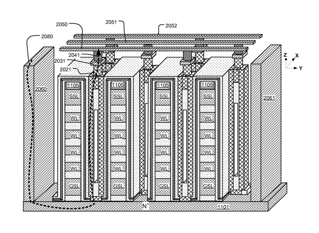
[0044]FIG. 1 is a schematic diagram of a three-dimensional 3D memory device 100 having an independent double gate, vertical channel structure, like that described in commonly owned, co-pending application Ser. No. 14 / 471,788, filed on 28 Aug. 2014, which application is incorporated by reference as if fully set forth herein.

[0045]The memory device 100 includes an array of NAND strings of memory cells, configured in an independent double gate vertical channel memory array (IDGVC) with two NAND strings per vertical channel, and suitable for multiple-bit-per-cell data storage. The memory device 100 includes an integrated circuit substrate, and a plurality of stacks of conductive strips separated by insulating material, including at least a bottom plane of conductive strips (GSL), a plurality of intermediate planes of conductive strips (WLs), and a top plane of conductive str...


PUM


Abstract

A memory device which can be configured as a 3D NAND flash memory, includes a plurality of stacks of conductive strips, including even stacks and odd stacks having sidewalls. Some of the conductive strips in the stacks are configured as word lines. Data storage structures are disposed on the sidewalls of the even and odd stacks. Active pillars between corresponding even and odd stacks of conductive strips include even and odd semiconductor films having outside surfaces and inside surfaces, the outside surfaces disposed on the data storage structures on the sidewalls of the corresponding even and odd stacks in the plurality of stacks forming a 3D array of memory cells, the inside surfaces are separated by an insulating structure that can include a gap. The semiconductor films can be thin-films.

Description

BACKGROUND OF THE INVENTION[0001]This application is related to co-pending U.S. patent application Ser. No. 14 / 637,204, filed 03 Mar. 2015, entitled U-SHAPED VERTICAL THIN-CHANNEL MEMORY.[0002]Field of the Invention[0003]The present invention relates to high density memory devices, and particularly to memory devices in which multiple planes of memory cells are arranged to provide a three-dimensional 3D array.[0004]Description of Related Art[0005]As critical dimensions of devices in integrated circuits shrink to the limits of common memory cell technologies, designers have been looking to techniques for stacking multiple planes of memory cells to achieve greater storage capacity, and to achieve lower costs per bit. For example, thin-film transistor techniques are applied to charge trapping memory technologies in Lai, et al., “A Multi-Layer Stackable Thin-Film Transistor (TFT) NAND-Type Flash Memory,” IEEE Int'l Electron Devices Meeting, 11-13 Dec. 2006; and in Jung et al., “Three Dim...

Claims


Application Information

Patent Timeline
Patent Type & Authority Patents(United States)
IPC IPC(8): G11C16/04H01L29/51H01L29/06H01L29/66H01L27/11565H01L29/786H01L27/11582H01L27/1157
CPCH01L27/11582H01L27/1157H01L27/11565H01L29/0649H01L29/511H01L29/66742H01L29/786G11C16/0483H10B43/35H10B43/10H10B43/27
Inventor LUE, HANG-TING
Owner MACRONIX INT CO LTD
Why Eureka
Try Eureka