Sacrificial spin-on glass for air gap formation after bl isolation process in single gate vertical channel 3D NAND flash

a technology of nand flash and sacrificial spin, which is applied in the direction of semiconductor devices, instruments, electrical equipment, etc., can solve the problems of uneven deep hole etching process through the insulating material, negative device performance, and non-uniform device structure, so as to improve the regularity of profiles and reduce the deformation of deep holes

Active Publication Date: 2016-07-26
MACRONIX INT CO LTD
View PDF34 Cites 41 Cited by
  • Summary
  • Abstract
  • Description
  • Claims
  • Application Information

AI Technical Summary

Benefits of technology

[0010]A method of manufacture of a vertical thin-channel memory is described, where the thin-channel memory can be configured as a 3D NAND flash memory. Vertical thin-channel cells in the memory are arranged along vertical active pillars which comprise U-shaped semiconductor thin-films, providing a structure with semiconductor thin-films on two sides electrically separated along the length of the pillar and electrically connected at the bottom. The active pillars are disposed between stacks of conductive strips operable as word lines with memory elements in between. As a result of this structure, two memory cells are formed per frustum of the active pillar, where each memory cell at the frustum includes a channel in the semiconductor thin-film on one side of the active pillar. The array can be configured, in addition, for multiple-bit-per-site operation. A NAND string of series connected memory cells can be provided that includes the memory cells along the U-shaped path of a single active pillar. The method of manufacture includes forming steps which improve the regularity of the profiles and reduce deformities of deep holes created for the formation of the U-shaped semiconductor films.

Problems solved by technology

However, because the insulation material includes a gap, the deep hole etching process through the insulating material may not be uniform.
This non-uniformness may cause irregular profiles and deformities of the deep holes and therefore non-uniformness in the resulting structures of the device.
These irregularities and deformities are not desirable because they may result negatively on device performance.

Method used


Image

  • Sacrificial spin-on glass for air gap formation after bl isolation process in single gate vertical channel 3D NAND flash
  • Sacrificial spin-on glass for air gap formation after bl isolation process in single gate vertical channel 3D NAND flash
  • Sacrificial spin-on glass for air gap formation after bl isolation process in single gate vertical channel 3D NAND flash

Examples


Embodiment Construction

[0069]A detailed description of embodiments of the present invention is provided with reference to the FIGS. 1-27.

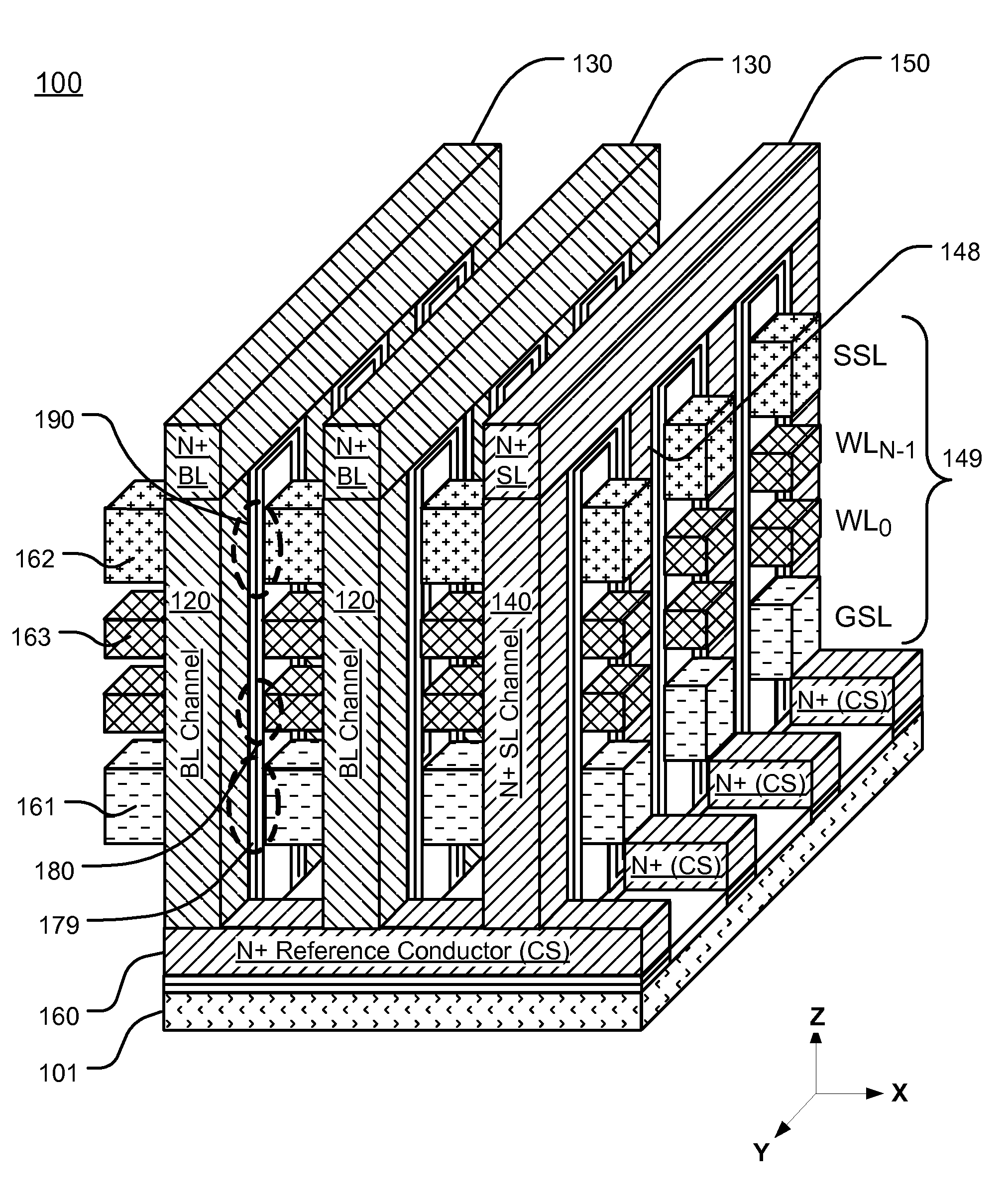
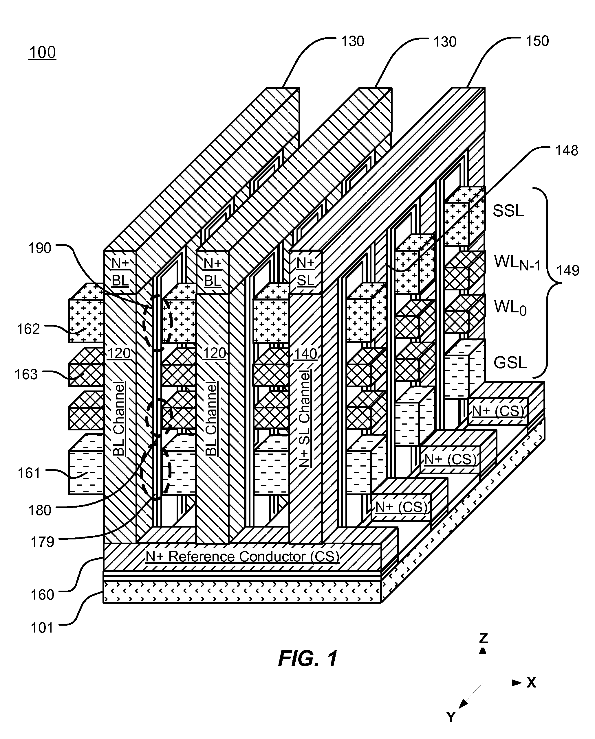
[0070]FIG. 1 is a schematic diagram of a three-dimensional 3D memory device 100 having an independent double gate structure according to a 3D vertical channel technology having a structure as described in co-pending U.S. patent application Ser. No. 14 / 471,788, filed on 28 Aug. 2014, [MXIC 2092-2] which application is incorporated by reference as if fully set forth herein.

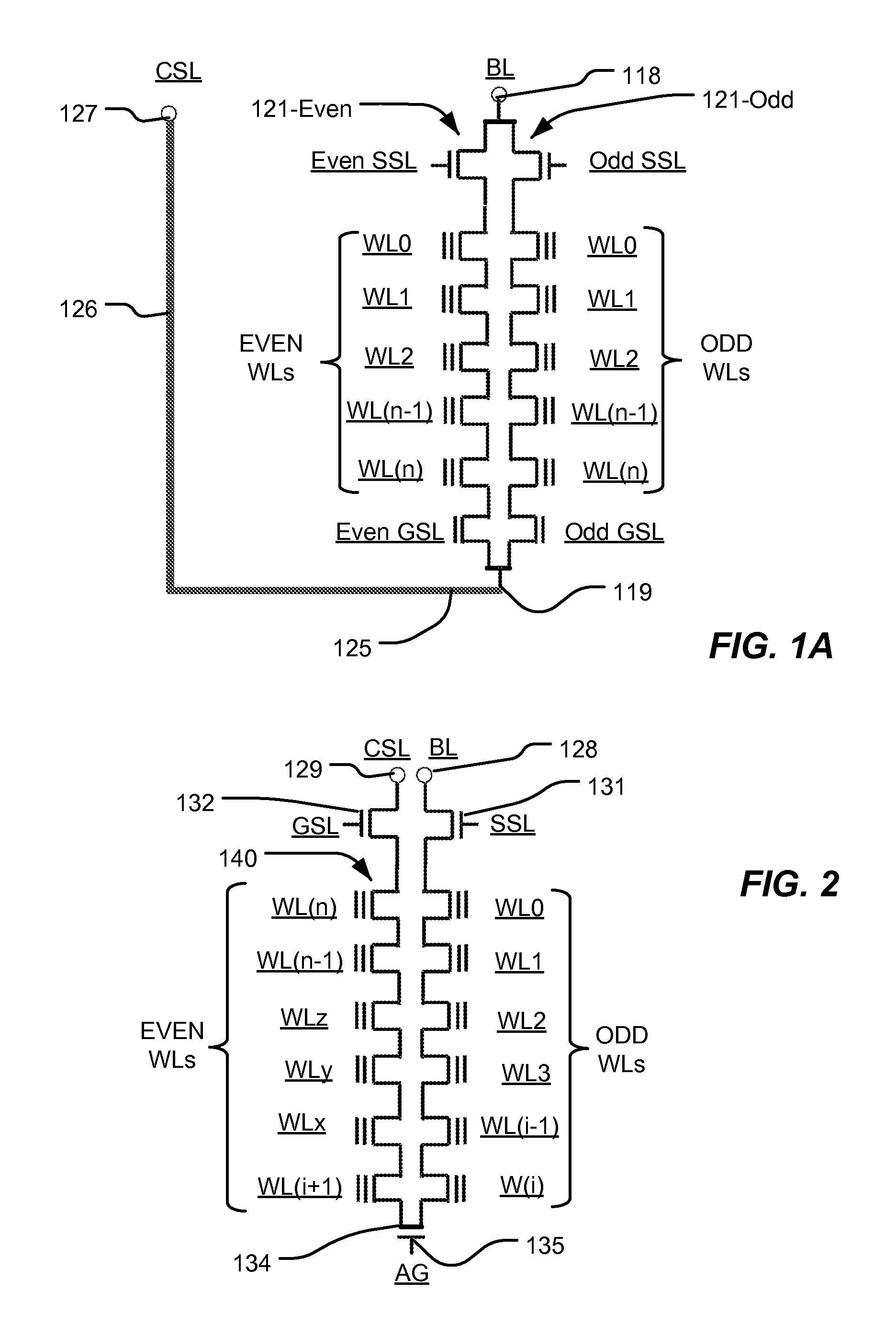
[0071]The memory device 100 includes an array of NAND strings of memory cells, configured in an independent double gate vertical channel memory array (IDGVC) with two NAND strings per vertical channel, and suitable for multiple-bit-per-cell data storage. The memory device 100 includes an integrated circuit substrate, and a plurality of stacks of conductive strips separated by insulating material, including at least a bottom plane of conductive strips (GSL), a plurality of intermediate planes of conductiv...


PUM


Abstract

A method for manufacturing a memory device, which can be configured as a 3D NAND flash memory, and includes a plurality of stacks of conductive strips, including even stacks and odd stacks having sidewalls. Some of the conductive strips in the stacks are configured as word lines. Data storage structures are disposed on the sidewalls of the even and odd stacks. Active pillars between corresponding even and odd stacks of conductive strips include even and odd semiconductor films connected at the bottom of the trench between the stacks, and have outside surfaces and inside surfaces. The outside surfaces contact the data storage structures on the sidewalls of the corresponding even and odd stacks forming a 3D array of memory cells; the inside surfaces are separated by an insulating structure that can include a gap. The semiconductor films can be thin-films having a U-shaped current path.

Description

BACKGROUND OF THE INVENTION[0001]1. Field of the Invention[0002]The present invention relates to high density memory devices, and particularly to memory devices in which multiple planes of memory cells are arranged to provide a three-dimensional 3D array.[0003]2. Description of Related Art[0004]The subject matter discussed in this section should not be assumed to be prior art merely as a result of its mention in this section. Similarly, a problem mentioned in this section or associated with the subject matter provided as background should not be assumed to have been previously recognized in the prior art. The subject matter in this section merely represents different approaches, which in and of themselves can also correspond to implementations of the claimed technology.[0005]As critical dimensions of devices in integrated circuits shrink to the limits of common memory cell technologies, designers have been looking to techniques for stacking multiple planes of memory cells to achieve...

Claims


Application Information

Patent Timeline
Patent Type & Authority Patents(United States)
IPC IPC(8): H01L21/336H01L29/76G11C16/04H01L27/115H01L21/28H01L21/311H01L21/768H01L21/764H01L29/06
CPCH01L27/11582H01L27/1157H01L21/28282H01L21/31111H01L21/768H01L21/764H01L29/0649H10B43/35H10B43/20H10B43/10H10B43/27
Inventor LEE, GUAN-RUCHIU, CHIAJUNG
Owner MACRONIX INT CO LTD
Why Eureka
Try Eureka