Supercharge Your Innovation With Domain-Expert AI Agents!

Light emitting device

a technology light source, which is applied in the direction of semiconductor devices, basic electric elements, electrical apparatus, etc., can solve the problems of deterioration of light emitting device members (e.g. resin) by ultraviolet radiation, complex construction or control means of light emitting device, and high operational cost, etc., to achieve high color purity and reduce ultraviolet radiation deterioration possibility

Active Publication Date: 2017-07-04
NICHIA CORP
View PDF33 Cites 0 Cited by
  • Summary
  • Abstract
  • Description
  • Claims
  • Application Information

AI Technical Summary

Benefits of technology

The patent text describes a device that reduces the risk of fading from exposure to sunlight. This means that the device can produce high-quality, pure red light in a small size.

Problems solved by technology

Accordingly, the construction or control means of the light emitting device will be very complicated.
As a result, the device itself, and its operational cost may be expensive.
For example, as a light emitting device which includes a light emitting element and a phosphor, and emits red light, in the case where a light emitting device includes a light emitting element that emits light containing ultraviolet radiation, and a phosphor that is excited by the ultraviolet radiation, there is a possibility that some members (e.g., resin) of the light emitting device may be deteriorated by the ultraviolet radiation.
In particular, in the case where this type of light emitting device is small, the amount of the phosphor may not be enough to sufficiently absorb light from the light emitting element since the space of the small light emitting device is limited.
As a result, there is a problem that the expected color purity of the monochromatic red light emitting device is not achieved.
On the other hand, in particular, in the case where a light emitting device is small, the space of the small light emitting device is limited for accommodating the phosphor, that is, a sufficient amount of the phosphor for emitting red light may not be accommodated.
As a result, the red color purity of the light emitting device may be insufficient for a red monochromatic light emitting device.

Method used


Image

  • Light emitting device
  • Light emitting device
  • Light emitting device

Examples


second embodiment

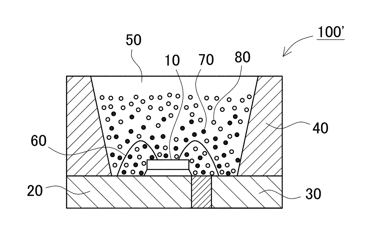
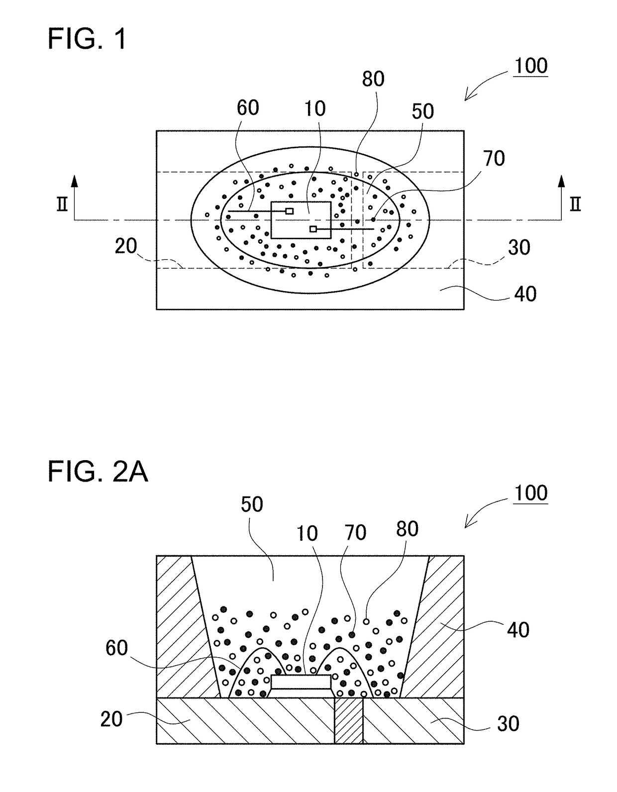
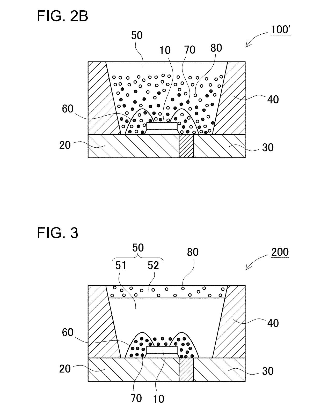
[0065]It has been described that the red phosphor 70 and the pigment 80 are mixed and distributed in the common sealing member 50 in the light emitting device 100 according to the first embodiment shown in FIGS. 1 and 2A. However, the present invention is not limited to this. The phosphor and the pigment can be included in separated sealing members. This type of light emitting device according to a second embodiment is shown in a cross-sectional view of FIG. 3. In the illustrated light emitting device 200, the sealing member 50 is constructed of a first sealing portion 51 which contains the phosphor 70, and a second sealing portion 52 which contains the pigment 80. In particular, it is preferable that the first sealing portion 51 covers the light emitting element 10, and the second sealing portion 52 covers the first sealing portion 51. Since the phosphor 70 and the pigment 80 are physically separated from each other, and the first sealing portion 51 which includes the phosphor 70 i...

third embodiment

[0066]The arrangement of the first and second sealing portions is not limited to the arrangement shown in FIG. 3. Various suitable arrangements can be used for the first and second sealing portions. For example, an angled part is formed on the upper part of the side wall of the molded member 40 in a light emitting device 300 according to a third embodiment shown in FIG. 4. This angled part can be easily formed by changing the inclination of the side wall. The part of the recessed part lower than the angled part is filled with the first sealing portion 51 in which the phosphor 70 is settled. The second sealing portion 52 which includes the pigment 80 is arranged on the first sealing portion 51. According to this arrangement, the second sealing portion 52 can be easily fastened to the upper part of the molded member 40, and is less likely to be removed.

fourth embodiment

[0067]The first sealing portion 51 which includes the phosphor 70 is substantially coplanar with the top surface of the side wall of the molded member 40 after the recessed part of the molded member 40 is filled with the first sealing portion 51, and the second sealing portion 52 which includes the pigment 80 is arranged on the top surfaces of the first sealing portion 51 and the side wall of the molded member 40 in a light emitting device 400 according to a fourth embodiment shown in FIG. 5.


PUM


Abstract

A light emitting device is provided which includes a light emitting element, a phosphor, and a sealing member. The light emitting element has a light emission peak wavelength in the range not shorter than 400 nm and not longer than 460 nm. The phosphor can be excited by light from the light emitting element, and emit luminescent radiation with a light emission peak wavelength in the range in not shorter than 600 nm and not longer than 700 nm. The sealing member includes a pigment for absorbing a part of the light from the light emitting element. X of the light emission chromaticity of the light emitting device falls within the range of x≧0.600 in the chromaticity coordinates in the CIE 1931 color space chromaticity diagram.

Description

CROSS-REFERENCE TO RELATED APPLICATIONS[0001]The present application claims priority under 35 U. S. C. §119 to Japanese Patent Application No. 2014-223,519, filed Oct. 31, 2014, and No. 2015-166,277, filed Aug. 25, 2015. The contents of these applications are incorporated herein by reference in their entirety.BACKGROUND OF THE INVENTION[0002]1. Field of the Invention[0003]The present disclosure relates to a light emitting device that includes a light emitting element together with a phosphor.[0004]2. Description of the Related Art[0005]In recent years, light emitting diodes (hereinafter also referred to as LEDs), which provide substantial energy savings, are widely used as light emitting elements. In addition, a light emitting device includes a semiconductor light emitting element containing gallium nitride (GaN) and a yellow phosphor which is excited by light from this light emitting element and emits yellow luminescent radiation. This light emitting device can emit white range lig...

Claims


Application Information

Patent Timeline
Patent Type & Authority Patents(United States)
IPC IPC(8): H01L33/50H01L33/54
CPCH01L33/502H01L33/54H01L2224/48247H01L2224/48257H01L2224/73265H01L2224/8592H01L2933/0091
Inventor HOSOKAWA, SHOJIMIYAMOTO, KIMIHIROIWAKURA, DAISUKE
Owner NICHIA CORP
Features
  • R&D
  • Intellectual Property
  • Life Sciences
  • Materials
  • Tech Scout
  • Unparalleled Data Quality
  • Higher Quality Content
  • 60% Fewer Hallucinations
Learn More