Digital perceptron

a digital signal and perceptron technology, applied in the field of digital signal processors, can solve the problems of increasing the energy and processing time consumed by digital processors, and the energy and time consumed for searching a digital symbol by addresses in a large memory database storage become very inefficien

Active Publication Date: 2017-09-05
FLASHSILICON
View PDF14 Cites 7 Cited by
  • Summary
  • Abstract
  • Description
  • Claims
  • Application Information

AI Technical Summary

Benefits of technology

[0011]To fulfill the above described functions of digital perceptrons, we have applied the configurable non-volatile content memory array for storing the non-volatile digital content symbols (U.S. patent application Ser. No. 14 / 596,886, the disclosure of which is incorporated herein by reference in its entirety), and the Complementary Electrical Erasable Programmable Read Only Memory (CEEPROM) array disclosed in U.S. Pat. No. 8,817,546 B2 (the disclosure of which is incorporated herein by reference in its entirety) for storing the perceptive non-volatile digital symbols, to form the main portion of the digital perceptron. The digital perceptron 200 is shown in FIG. 2. In the digital perceptron 200, an n-bit×m-row non-volatile content memory array 600 through “2n” input lines 205 is connected to an n-bit input buffer and driver unit 700 with the connection of external n-bit input bus lines 250. When the “enabled high” signal at node 210 is activated by VDD, the input buffer and driver unit 700 receives the digital symbol signals from the external n-bit input bus lines 250 and broadcasts the n-bit digital signals into the n-bit×m-row non-volatile content memory array 600. The “m” rows of the match-lines 203 in the non-volatile content memory array 600 attach to a match detector 800 connected to the correspondent m-row wordlines of the q-bit×m-row CEEPROM array 100 by the “m” switching lines 204. When the m-row match detector 800 is activated by the “enabled high” VDD signal at node 210, the “matching” signal from one of the m match detector cells 850 in the match detector 800 can switch on the correspondent wordline in the q-bit×m-row CEEPROM array 100. The q-bit output signals by the “q” output lines 206 are then sent to the q-bit output buffer and driver unit 110. Meanwhile the “matching” signal from one of the m match detector cells 850 is also fed into the match logic circuitry 900 to generate the “send high” VDD signal at the node 208 for connecting the q-bit output buffer and driver unit 110 with the external q-bit output bus lines 251 to send out the q-bit output signals. On the other hand, if the n-bit input data does not match any row of the configured non-volatile data in the non-volatile content memory array 600, the output buffer and driver unit 110 are not connected to the external output bus lines 251. The digital perceptron 200 then sends no digital signals out to the external output bus lines 251. This function is to imitate the information processing by biological nerve systems in response to the irrelevant information inputs from the environments.
[0012]The “inhibition” function can be commonly observed for the neural networks in biologic nerve systems. One classic example is the knee jerk case, where the combination of excitatory and inhibitory synaptic connections mediating the stretch reflex of the quadriceps muscles. To imitate this function, we apply a simple “AND” gate 209 having two input nodes, an “Enable” node 252 and an “Inhibition” node 253, for turning on and off the digital perceptron 200. The digital perceptron 200 is turned on by the “enable high” VDD signal at the node 210, if and only if for the “high” VDD signal at the “Enable” node 252 and the “low” VSS signal at the “Inhibition” node 253.

Problems solved by technology

The more frequent memory accessing to complete the computation processing steps, the more energy and processing time are consumed for the digital processors.
The energy and time consumed for searching a digital symbol by addresses in a large memory database storage become very inefficient as the general practice of running programmed software algorithm with many times of memory accessing between CPU and non-volatile memory database storage, and the data comparisons in the present computing system.

Method used


Image

  • Digital perceptron
  • Digital perceptron
  • Digital perceptron

Examples


Embodiment Construction

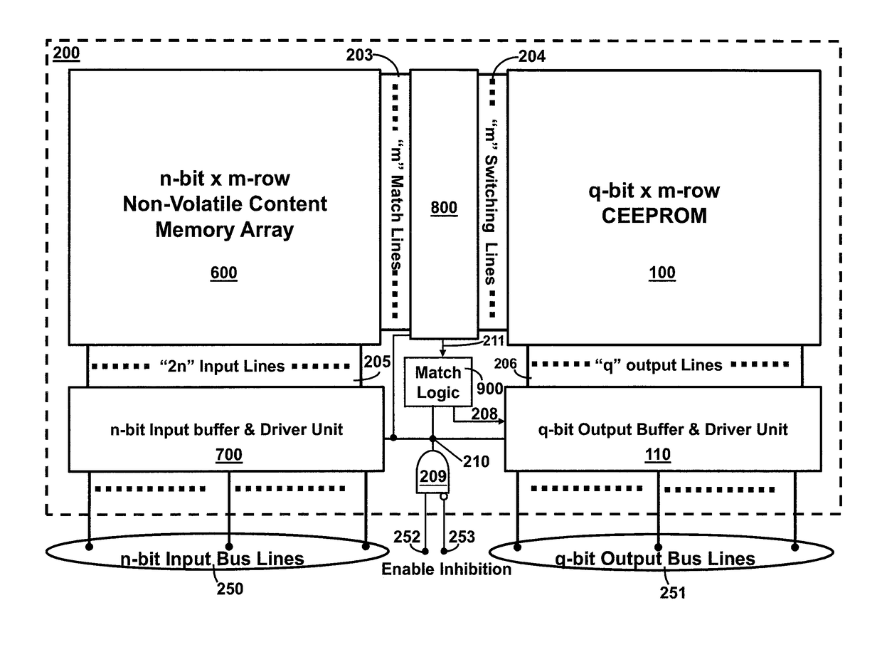
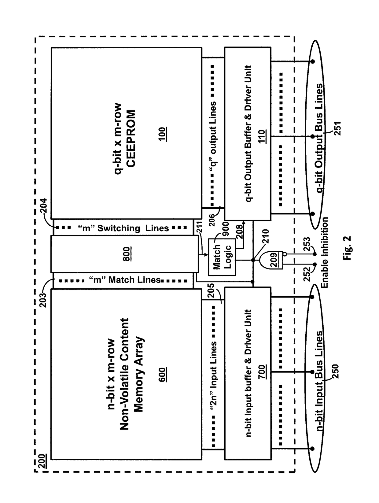
[0025]The following detailed description is meant to be illustrative only and not limiting. It is to be understood that other embodiment may be utilized and element changes may be made without departing from the scope of the present invention. Also, it is to be understood that the phraseology and terminology used herein are for the purpose of description and should not be regarded as limiting. Those of ordinary skill in the art will immediately realize that the embodiments of the present invention described herein in the context of methods and schematics are illustrative only and are not intended to be in any way limiting. Other embodiments of the present invention will readily suggest themselves to such skilled persons having the benefits of this disclosure. In the figures of the accompanying drawings, elements having the same reference numeral designations represent like elements throughout.

[0026]In one embodiment, the complementary Non-Volatile Memory (NVM) devices 310 and 320 ha...


PUM


Abstract

In view of the neural network information parallel processing, a digital perceptron device analogous to the build-in neural network hardware systems for parallel processing digital signals directly by the processor's memory content and memory perception in one feed-forward step is disclosed. The digital perceptron device of the invention applies the configurable content and perceptive non-volatile memory arrays as the memory processor hardware. The input digital signals are then broadcasted into the non-volatile content memory array for a match to output the digital signals from the perceptive non-volatile memory array as the content-perceptive digital perceptron device.

Description

BACKGROUND OF THE INVENTION[0001]Field of the Invention[0002]The invention is related to a digital signal processor, which can interpret the receptive digital signals into the perceptive output digital signals. In particular, the processor parallel processes digital information according to its pre-configured digital content and perceptive non-volatile memories without executing any sequential Boolean logic operations. That is, instead of executing the combinational logic computations given by the programmed instructions in the conventional digital processors, the invented digital signal processor intelligently processes digital information fully based on their configured content and perceptive non-volatile memory hardware.[0003]Description of the Related Art[0004]In the modern Von Neumann computing architecture as shown in FIG. 1, the Central Process Unit (CPU) executes logic operations according to the instructions and data from the main memory 11. The CPU 10 includes a main memor...

Claims


Application Information

Patent Timeline
Patent Type & Authority Patents(United States)
IPC IPC(8): G11C15/04G06F12/1036G11C15/00G06F12/1027G11C5/06G11C7/22G06F12/10
CPCG11C7/22G11C5/06G06F12/1027G11C15/00G11C15/046G06F12/10G06F12/1036G11C15/04G06N3/063G11C11/005G11C11/54G11C13/0002
Inventor WANG, LEE
Owner FLASHSILICON
Why Eureka
Try Eureka