
Electronic device, and method for manufacturing electronic device

a technology of electronic devices and manufacturing methods, applied in the field of electronic devices, can solve the problems of lowered patterning accuracy, and insufficient adhesive strength of photosensitive resins, etc., and achieve the effect of accurately applying a predetermined amoun

Active Publication Date: 2017-10-17
SEIKO EPSON CORP
View PDF13 Cites 0 Cited by
  • Summary
  • Abstract
  • Description
  • Claims
  • Application Information

AI Technical Summary

Benefits of technology

The patent text describes a method to improve the accuracy and reliability of patterning and adhesion in a photosensitive resin used in electronic devices. By using an adhesive agent and a low viscosity resin, the method prevents the reinforcement resin from spreading and allows for closer proximity between the bonding resin and the substrate, resulting in higher density and miniaturization of the electronic device. Additionally, the method allows for accurate application of the reinforcement resin at predetermined positions. Overall, the method improves the stability and yield rate of electronic device manufacturing.

Problems solved by technology

However, if the photosensitive resin 53 is not cured to a certain degree at the time of the developing, there is concern that the photosensitive resin 53 is peeled off from the substrate or the shape collapses, or there is a problem that patterning accuracy is lowered.
On the other hand, since the curing of the photosensitive resin 53 proceeds by the heat treatment in this manner, in the state where the substrates are bonded to each other as illustrated in FIG. 8C and FIG. 8D, there are problems that an adhesive strength of the photosensitive resin 53 is insufficient, and adhesion reliability is lowered.

Method used


Image

  • Electronic device, and method for manufacturing electronic device
  • Electronic device, and method for manufacturing electronic device
  • Electronic device, and method for manufacturing electronic device

Examples


Embodiment Construction

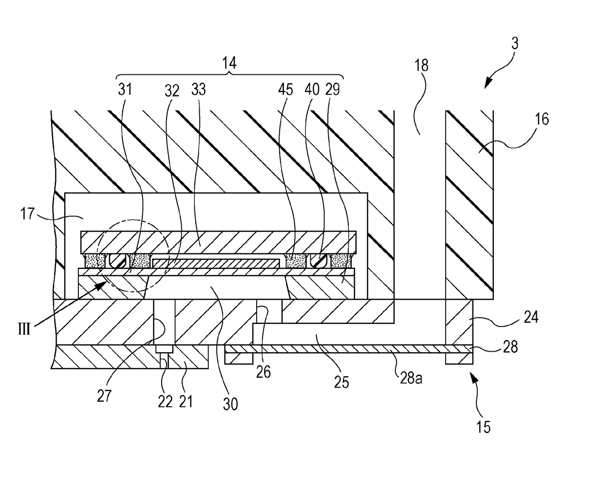
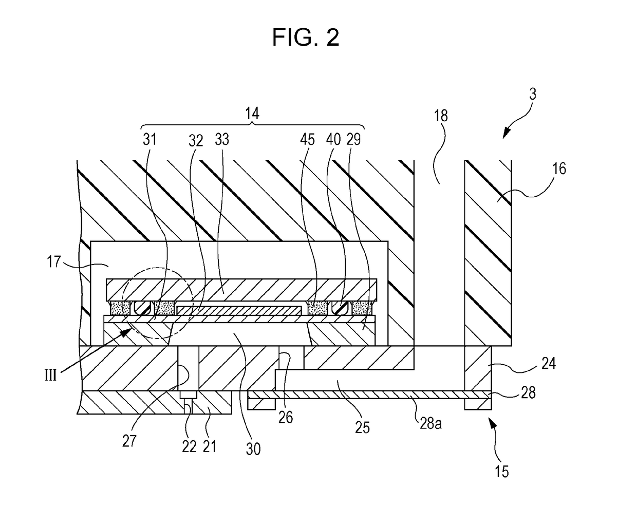
[0028]Hereinafter, modes for carrying out the invention will be described with reference to the accompanying drawings. Embodiments described below are variously limited as a suitable specific example of the invention, but unless the gist of particularly limiting the invention is written in the following description, the scope of the invention is not limited to the embodiments. Moreover, in the following description, an ink jet type printer (hereinafter, printer) being one type of liquid ejecting apparatus on which an ink jet type recording head (hereinafter, recording head) being one type of liquid ejecting head including an electronic device according to an embodiment of the invention is mounted, will be described by being used as an example.

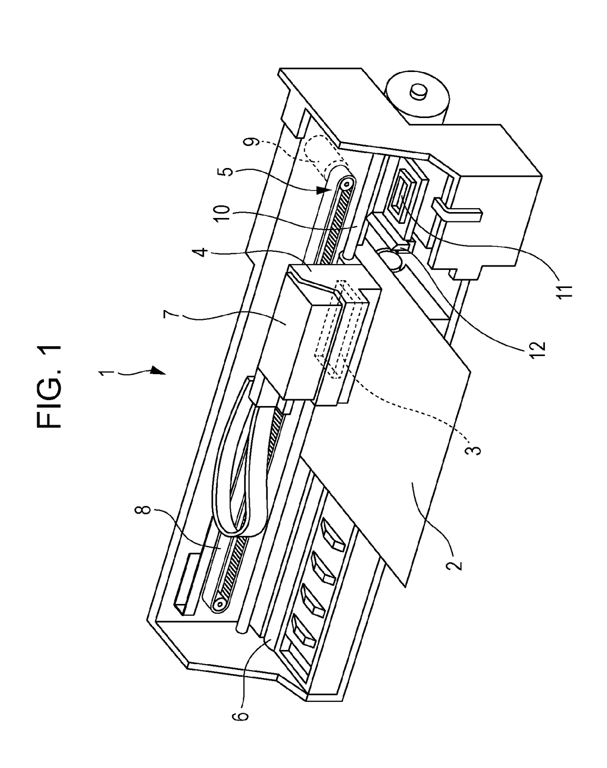
[0029]A configuration of a printer 1 will be described with reference to FIG. 1. The printer 1 is an apparatus that performs a recording of an image or the like by ejecting and discharging an ink (one type of liquid) onto a surface of a recordi...


PUM


Abstract

A bonding resin that bonds substrates to each other in a state of being spaced with a gap between the substrates is configured by stacking a photosensitive resin and a bonding reinforcement resin which is different from the photosensitive resin, the photosensitive resin is patterned in one substrate, and the bonding reinforcement resin which is stacked on the patterned photosensitive resin has a fillet being a wet-spreading portion or a portion which swells outward from the photosensitive resin.

Description

[0001]The entire disclosure of Japanese Patent Application No: 2015-052889, filed Mar. 17, 2015 is expressly incorporated by reference herein in its entirety.BACKGROUND[0002]1. Technical Field[0003]The present invention relates to an electronic device where a first substrate and a second substrate are bonded to each other in a state of interposing a bonding resin having photosensitivity between the first substrate and the second substrate, and a method for manufacturing the same.[0004]2. Related Art[0005]An electronic device is a device including a drive element such as a piezoelectric element which is deformed by applying a voltage, and is applied to various types of apparatuses or sensors. For example, in a liquid ejecting apparatus, various types of liquids are ejected from a liquid ejecting head using the electronic device. As such a liquid ejecting apparatus, for example, there is an image recording apparatus such as an ink jet type printer or an ink jet type plotter, but recen...

Claims


Application Information

Patent Timeline
Patent Type & Authority Patents(United States)
IPC IPC(8): B41J2/16B41J2/14
CPCB41J2/1623B41J2/14B41J2/14201B41J2/14233B41J2/161B41J2/1607B41J2/1631B41J2002/14419B41J2002/14491H01L2224/2919H01L2224/29082
Inventor SATO, NAOYA
Owner SEIKO EPSON CORP
Learn More