
Manufacturing method of electronic device, electronic device, electronic apparatus, and moving body

a manufacturing method and technology of electronic devices, applied in the direction of fluid speed measurement, instruments, coatings, etc., can solve the problems of reduced bonding strength of lids and base bodies, uneven size of even portions, and reduced flatness, so as to enhance the bonding strength of first base body and third base body, stabilize the bonding, and improve reliability

Active Publication Date: 2017-10-24
SEIKO EPSON CORP
View PDF22 Cites 1 Cited by
  • Summary
  • Abstract
  • Description
  • Claims
  • Application Information

AI Technical Summary

Benefits of technology

[0009]According to the application example, even if the first etching process is performed on the second base body, which is bonded (a first repetition) to the first base body using the protective layer, which is provided on the first base body to which the third base body is to be bonded, it is possible to suppress a circumstance in which the outer surface of the first base body, to which the third base body is to be bonded, becomes rough, uneven portions are increased in size, and flatness is impaired as a result. Further, it is possible to sufficiently perform bonding of the first base body and the third base body by bonding the third base body to the first base body (a surface in which flatness is not impaired) from which the protective layer was removed. In other words, it is possible to suppress a circumstance in which the bonding strength of the first base body and the third base body is reduced, the bonding state is unstable, or the like, due to the flatness of the first base body being impaired.
[0022]According to the application example, a second surface having a more pronounced rough surface state than the first surface is provided in a peripheral region of the first surface, which includes a bonding portion of the first base body and the third base body. In other words, the first surface, which includes the bonding portion of the first base body and the third base body, is configured so that the surface roughness thereof is less than that of the peripheral region thereof. Accordingly, it is possible to stabilize the bonding of the first base body and the third base body, and therefore, it is also possible to increase the bonding strength.
[0031]According to the application example, since the moving body is provided with an electronic device in which the bonding strength of the first base body and third base body is enhanced and stabilized bonding is performed, it is possible to configure a moving body in which reliability is improved.

Problems solved by technology

However, when, in the manner disclosed in JP-A-2013-164285, an etching process for forming a functional element is performed after anodic bonding (a first repetition) of a base body and a silicon substrate, which corresponds to the functional element, the outer surface of the substrate on which a second repetition of anodic bonding is performed becomes rough, uneven portions are increased in size, and therefore, flatness is impaired.
When an attempt is made to anodically bond (a second repetition) a lid to an outer surface of a substrate in which flatness is impaired in this manner, bonding of the lid and a base body is not performed sufficiently, consequently, the bonding strength of the lid and the base body is reduced, the bonding state is unstable, or the like, and there is a concern that the airtightness between the lid and the base body will be reduced as a result.
In other words, it is possible to suppress a circumstance in which the bonding strength of the first base body and the third base body is reduced, the bonding state is unstable, or the like, due to the flatness of the first base body being impaired.

Method used


Image

  • Manufacturing method of electronic device, electronic device, electronic apparatus, and moving body
  • Manufacturing method of electronic device, electronic device, electronic apparatus, and moving body
  • Manufacturing method of electronic device, electronic device, electronic apparatus, and moving body

Examples


embodiment

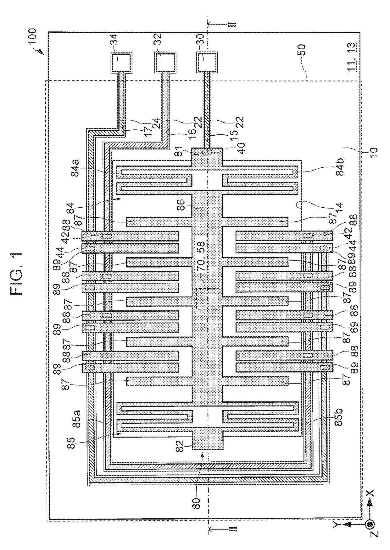
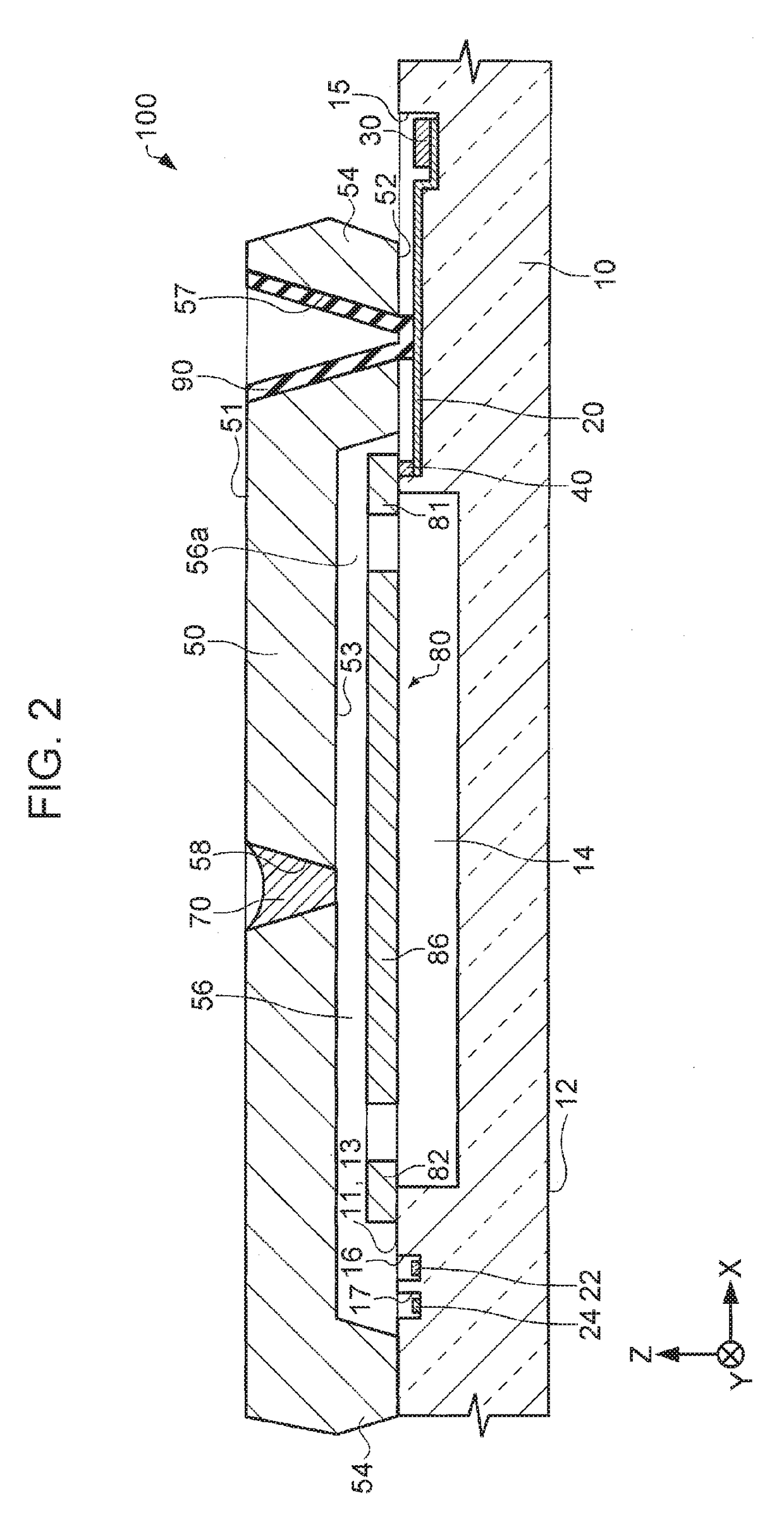
[0055]An electronic device and a manufacturing method of an electronic device according to the embodiment of the invention will be described using FIG. 1, FIG. 2, FIG. 3A, FIG. 3B, FIG. 4, FIG. 5A to FIG. 5F, FIG. 6 and FIG. 7. FIG. 1 and FIG. 2 schematically show an electronic device according to the embodiment of the invention, FIG. 1 is a plan view, and FIG. 2 is a front cross-sectional view along a line II-II in FIG. 1. FIG. 3A and FIG. 3B schematically show a bonding portion of a base body and a lid in the electronic device according to the present embodiment, FIG. 3A is a plan view, and FIG. 3B is a front cross-sectional view along a line IIIB-IIIB in FIG. 3A. FIG. 4 is a flowchart that shows an outline of a manufacturing method of an electronic device according to the present embodiment. FIG. 5A to FIG. 5F are process flow views that show the manufacturing method of an electronic device according to the present embodiment (front cross-sectional views that schematically show t...

modification example 1

[0132]Next, Modification Example 1 of the manufacturing method of an electronic device will be described with reference to FIG. 8A, FIG. 8B and FIG. 8C. FIG. 8A is a process flow-1 (a front cross-sectional view) that shows an outline of a manufacturing method of an electronic device according to Modification Example 1. FIG. 8B is a process flow-2 (a front cross-sectional view) that shows the manufacturing method according to Modification Example 1. FIG. 8C is a process flow-3 (a front cross-sectional view) that shows the manufacturing method according to Modification Example 1.

[0133]In the manufacturing method of an electronic device according to Modification Example 1, the configuration of the silicon substrate 8, which is the functional element 80 as the third base body, differs from that of the manufacturing method of the electronic device 100 according to the above-mentioned embodiment. The description of the present Modification Example 1 will be given focusing on manufacturing...

modification example 2

[0141]Next, Modification Example 2 of a manufacturing method of an electronic device will be described with reference to FIG. 9. FIG. 9 is a front cross-sectional view that schematically shows a bonding portion of a base body and a lid of an electronic device according to Modification Example 2. In the manufacturing method of an electronic device according to the present Modification Example 2, the method of formation of protective layers 60a, which are provided on the outer surface 11 of the base body 10, differs from that of the above-mentioned embodiment. The description of other processes will be omitted since they are similar to those of the above-mentioned embodiment, and in this instance, the method of formation of protective layers 60a will be described.

[0142]As shown in FIG. 9, the protective layers 60a according to Modification Example 2 are install inside bottomed recessed sections 68, which is engraved into the outer surface 11 of the base body 10. The recessed sections ...


PUM

PropertyMeasurementUnit
temperatureaaaaaaaaaa
DC voltageaaaaaaaaaa

Abstract

A manufacturing method of an electronic device includes a process that forms a protective layer on at least a portion of the first base body to which a third base body is to be bonded, a process that performs first bonding of a second base body to the first base body, a process that performs a first etching of the second base body bonded by the first bonding, a process that removes the protective layer using a second etching, and a process that performs second bonding of the third base body to the first base body. In the first etching, an etching rate of the second base body is faster than those of the first base body and the protective layer, and in the second etching, an etching rate of the protective layer is faster than those of the first base body and the second base body.

Description

BACKGROUND[0001]1. Technical Field[0002]The present invention relates to a manufacturing method of an electronic device, an electronic device, an electronic apparatus, and a moving body.[0003]2. Related Art[0004]In the related art, for example, acceleration sensors, gyro sensors, and the like in which functional elements that are formed from silicon substrates, and the like, are provided on package substrates (base bodies) such as semiconductor substrates or glass substrates, have been proposed as electronic devices that are provided with functional elements which detect physical quantities using silicon Micro Electro Mechanical Systems (MEMS).[0005]For example, JP-A-2013-164285 discloses an electronic device, which is provided with a lid that is joined to a first surface side of a base body (equivalent to the above-mentioned package substrate) and a functional element (a sensor element) that is stored in a cavity, which is surrounded by the base body and the lid, and a manufacturin...

Claims


Application Information

Patent Timeline
Patent Type & Authority Patents(United States)
IPC IPC(8): B81B7/00B81C1/00
CPCB81B7/0051B81C1/00325B81C2203/031B81C2201/053B81C2201/013B81C1/00801B81C2201/019B81C2203/0109B81C2203/0145
Inventor TAKAGI, SHIGEKAZU
Owner SEIKO EPSON CORP
Learn More