Semiconductor layout generation

Inactive Publication Date: 2017-12-05
GLOBALFOUNDRIES US INC
View PDF7 Cites 3 Cited by
  • Summary
  • Abstract
  • Description
  • Claims
  • Application Information

AI Technical Summary

Benefits of technology

[0007]Such layout generation may also include generating, by the layout design module, a plurality of alternative layout. Each of the alternative layouts includes a variation of the interdependent chara

Problems solved by technology

Current methods to ensure that such layout can be fabricated without failure are often inefficient and sub-optimal.
Also, a layout may be compliant to an individual d

Method used


Image

  • Semiconductor layout generation
  • Semiconductor layout generation
  • Semiconductor layout generation

Examples


Embodiment Construction

)

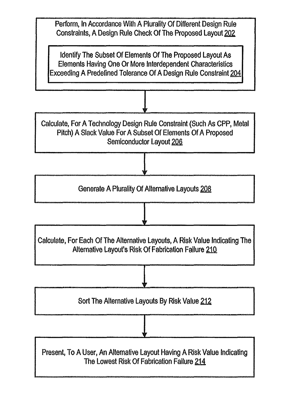
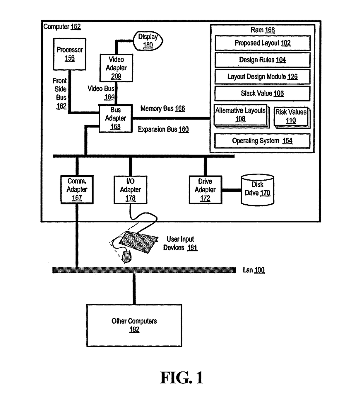
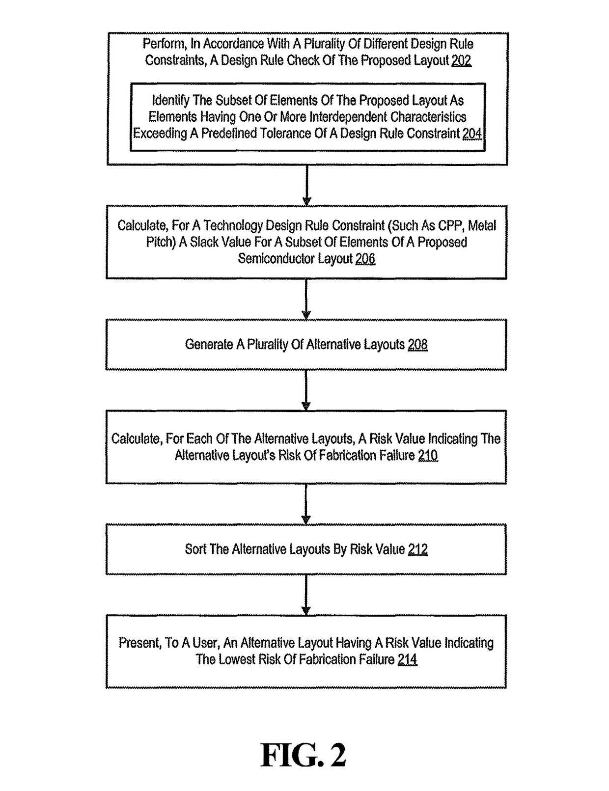
[0013]Example methods, apparatus, and products for semiconductor layout generation in accordance with embodiments are described herein with reference to the accompanying drawings, beginning with FIG. 1. FIG. 1 sets forth a network diagram of a system for semiconductor layout generation according to embodiments described herein. The system of FIG. 1 includes an example of automated computing machinery in the form of a computer (152). The computer (152) of FIG. 1 includes at least one computer processor (156) or ‘CPU’ as well as random access memory (168) (‘RAM’) which is connected through a high speed memory bus (166) and bus adapter (158) to processor (156) and to other components of the computer (152).

[0014]Stored in RAM (168) is a layout design module (126), a module of computer program instructions for semiconductor layout generation in accordance with embodiments described herein. A layout, as the term is used here, is a data structure comprising at least a structured descripti...


PUM


Abstract

Semiconductor layout generation includes: calculating, for a design rule constraint, a slack value for a subset of elements of a proposed semiconductor layout; generating a plurality of alternative layouts, where each of the alternative layouts includes a variation of interdependent characteristics of the subset of elements and a slack value for the subset of elements of each of the alternative layouts is less than the calculated slack value of subset of elements of the proposed layout; and calculating, by the layout design module for each of the alternative layouts, a risk value indicating the alternative layout's risk of fabrication failure.

Description

BACKGROUND OF THE INVENTION[0001]1. Field of the Invention[0002]The present disclosure is generally related to data processing, or, more specifically, methods, apparatus, and products for semiconductor layout generation.[0003]2. Description of Related Art[0004]Semiconductor circuits are generally brought into existence in two phases. In a first phase the circuit is designed. In a second phase, the circuit is fabricated on a semiconductor die. During the design phase, a circuit designer may create a layout of a circuit on a computer storage device to be used during the fabrication phase to fabricate the circuit on the silicon wafer.[0005]Current methods to ensure that such layout can be fabricated without failure are often inefficient and sub-optimal. For example, the fabrication process may be changed after the circuit design and layout are complete but before fabrication. Thus, the layout, if fabricated as originally designed, would result in sub-optimal yield in semiconductor manu...

Claims


Application Information

Patent Timeline
IPC IPC(8): G06F17/50
CPCG06F17/5072G06F17/5081G06F2119/18G06F30/392G06F30/398G06F30/39Y02P90/02
Inventor AZUMA, ATSUSHICUI, YUPINGCULP, JAMES A.FACCHINI, MARCOYAO, SHAONING
Owner GLOBALFOUNDRIES US INC
Why Eureka
Try Eureka