
Circuit board element

a technology of circuit board and element, applied in the direction of printed circuit, printed circuit manufacturing, printed circuit stress/warp reduction, etc., can solve the problems of circuit board element damage, unexpected problems, etc., to improve reduce the thickness and manufacturing cost of the circuit redistribution structure, and improve the effect of structure stability and wiring density

Active Publication Date: 2018-01-02
UNIMICRON TECH CORP
View PDF9 Cites 3 Cited by
  • Summary
  • Abstract
  • Description
  • Claims
  • Application Information

AI Technical Summary

Benefits of technology

The patent provides a way to make a circuit board that is more stable and has more wires without being too thick or expensive. The method also reduces the risk of the substrate breaking during the process. This makes the circuit board easier to use and more reliable.

Problems solved by technology

As these requirements of circuit boards continue, some unexpected problems may arise.
Since there may be small defects on the edges of the glass substrate due to the cutting process, the thermal stress applied to the glass substrate by the dielectric layer may break the glass substrate, such that the circuit board element may be damaged.

Method used


Image

  • Circuit board element
  • Circuit board element
  • Circuit board element

Examples


Embodiment Construction

[0026]In the following detailed description, for purposes of explanation, numerous specific details are set forth in order to provide a thorough understanding of the disclosed embodiments. It will be apparent, however, that one or more embodiments may be practiced without these specific details. In other instances, well-known structures and devices are schematically depicted in order to simplify the drawings.

[0027]Further, spatially relative terms, such as “beneath,”“below,”“lower,”“above,”“upper” and the like, may be used herein for ease of description to describe one element or feature's relationship to another element(s) or feature(s) as illustrated in the figures. The spatially relative terms are intended to encompass different orientations of the device in use or operation in addition to the orientation depicted in the figures. The apparatus may be otherwise oriented (rotated 90 degrees or at other orientations) and the spatially relative descriptors used herein may likewise be...


PUM

PropertyMeasurementUnit
thicknessaaaaaaaaaa
thicknessaaaaaaaaaa
width W1aaaaaaaaaa

Abstract

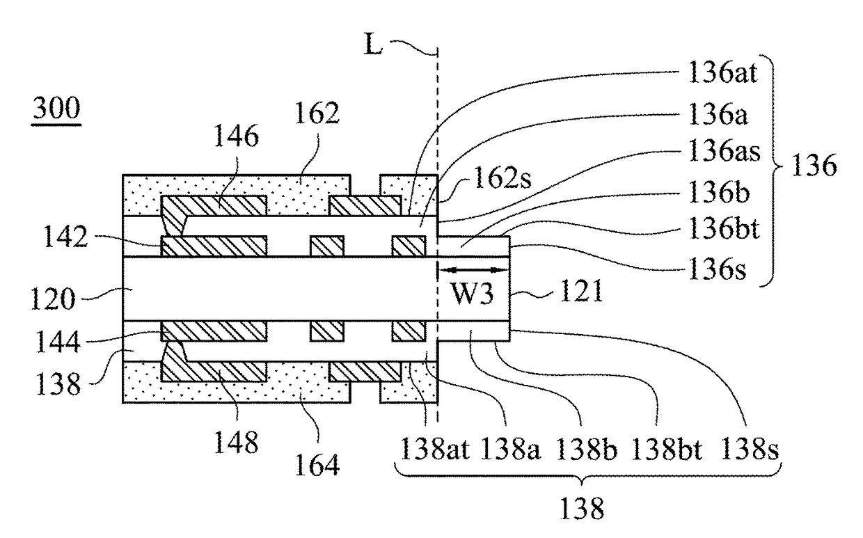
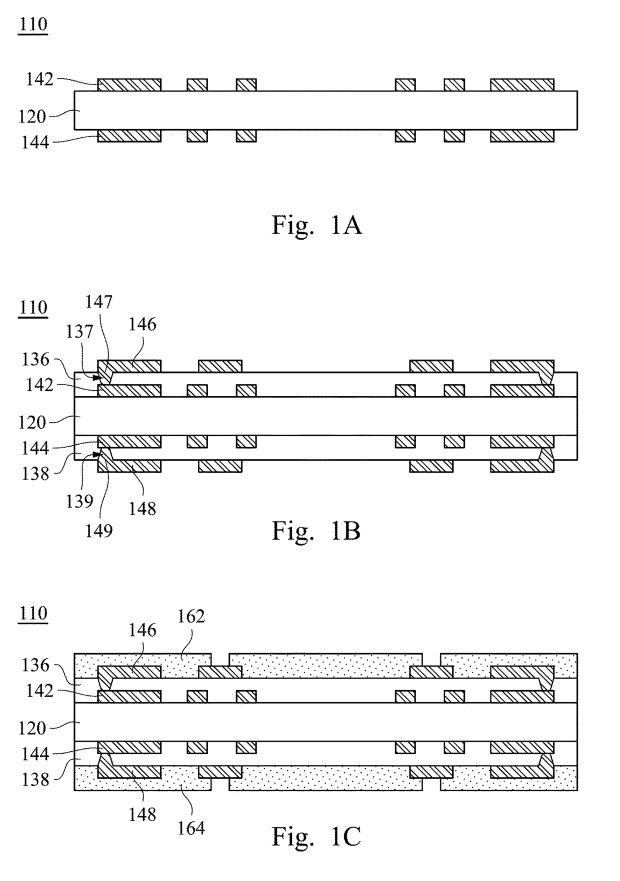
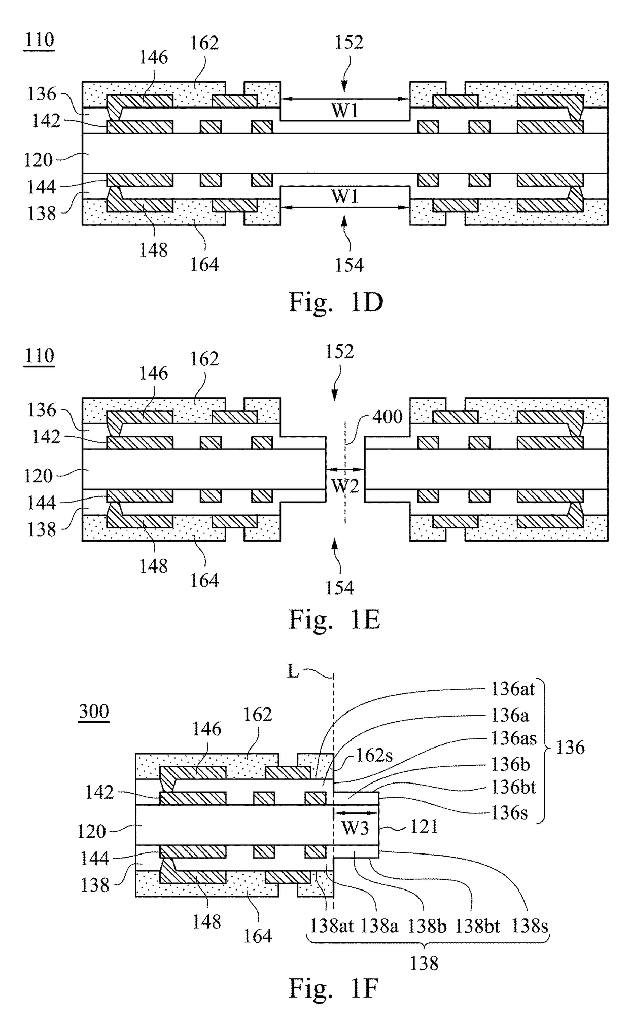
A circuit board element includes a glass substrate, a first dielectric layer, and a first patterned metal layer. The glass substrate has an edge. The first dielectric layer is disposed on the glass substrate and has a central region and an edge region. The edge region is in contact with the edge of the glass substrate, and the thickness of the central region is greater than the thickness of the edge region. The first patterned metal layer is disposed on the glass substrate and in the central region of the first dielectric layer.

Description

RELATED APPLICATIONS[0001]This application claims priority to Taiwanese Application Serial Number 105121258, filed Jul. 5, 2016, which are herein incorporated by reference.BACKGROUNDTechnical Field[0002]The present disclosure relates to a circuit board element.Description of Related Art[0003]With the rapid growth of the electronics industry, the R & D of electronic products has gradually been directed to the pursuit of versatility and high performance. In order to achieve the requirements of high integration and miniaturization of semiconductor components, the requirements of circuit boards also increase. For example, the line width and pitch of a circuit board is required to become smaller and smaller, and the thickness of the circuit board is required to become smaller and smaller. As these requirements of circuit boards continue, some unexpected problems may arise.[0004]To further improve the circuit boards, persons in the industry have made every endeavor to discover new solutio...

Claims


Application Information

Patent Timeline
Patent Type & Authority Patents(United States)
IPC IPC(8): H05K1/02H05K1/03
CPCH05K1/0306H05K1/0271H05K2201/0175H05K2201/068H05K2201/0154H05K3/0052H05K3/4605H05K3/4688H05K2201/09845
Inventor HSIEH, YU-CHUNGCHIEN, CHUN-HSIENLIN, WEI-TICHEN, YU-HUA
Owner UNIMICRON TECH CORP
Learn More