Comprehensive path based analysis process

a path analysis and path technology, applied in the field of electronic design automation, can solve the problems of inordinate turnaround time, overly burdensome storage, processing and memory requirements, and hindering efforts to minimize the cost of fabricated circuit products, time to market, power requirements,

Active Publication Date: 2018-01-23
CADENCE DESIGN SYST INC
View PDF10 Cites 39 Cited by
  • Summary
  • Abstract
  • Description
  • Claims
  • Application Information

AI Technical Summary

Benefits of technology

[0004]In one or more embodiments of the present disclosure, a computer-implemented method for comprehensive path based analysis in an electronic circuit design is provided. The method may include receiving, using at least one processor, an electronic design and determining one or more graph based analysis (“GBA”) violating nodes associated with the electronic design. Determining the one or more GBA violating nodes may include generating a timing graph associated with a given netlist and identifying a subset of nodes associated with the timing graph as GBA violating nodes. The method may include identifying a non-covered violating node from the GBA violating nodes and determining a worst timing path through the non-covered violating node. Embodiments may further include invoking a path-based analysis (“PBA”) on the worst timing path and determining if the worst timing path satisfies the PBA analysis.

Problems solved by technology

While signoff systems and methods are known, such heretofore known systems and methods are encumbered by numerous deficiencies.
Some of these include required repeated transformative iterations between timing signoff and physical implementation, highly divergent timing analysis between timing signoff and physical implementation optimizers—with highly pessimistic timing characteristics and attendant false-positive violations (requiring over-fixing), inordinate turnaround time, and overly burdensome storage, processing, and memory requirements.
Such deficiencies have hindered efforts to minimize fabricated circuit product cost, time to market, power requirements, and substrate area while maximizing performance.

Method used


Image

  • Comprehensive path based analysis process
  • Comprehensive path based analysis process
  • Comprehensive path based analysis process

Examples


Embodiment Construction

[0038]Reference will now be made in detail to the embodiments of the present disclosure, examples of which are illustrated in the accompanying drawings. The present disclosure may, however, be embodied in many different forms and should not be construed as being limited to the embodiments set forth herein. Rather, these embodiments are provided so that this disclosure will be thorough and complete, and will fully convey the concept of the disclosure to those skilled in the art.

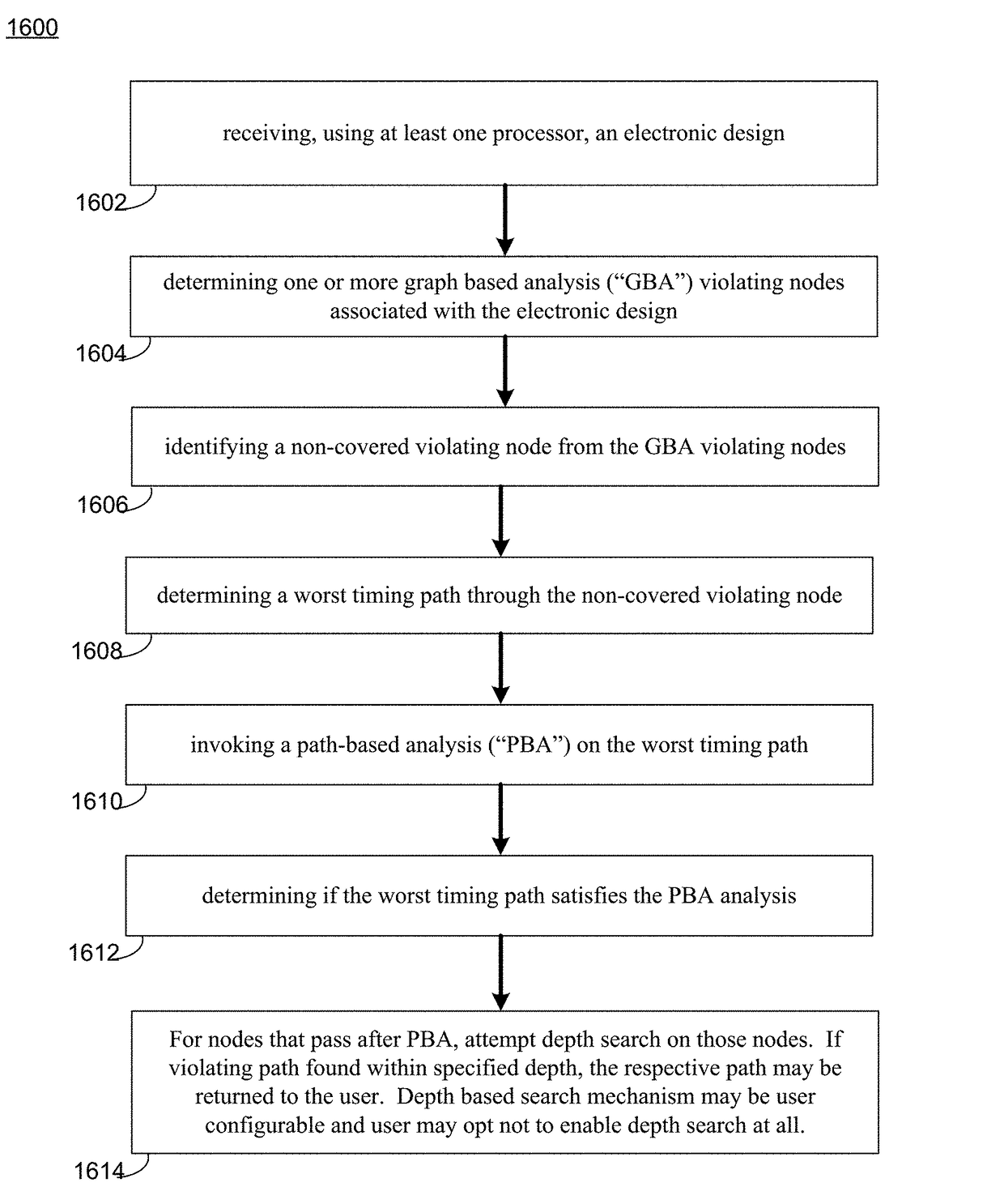
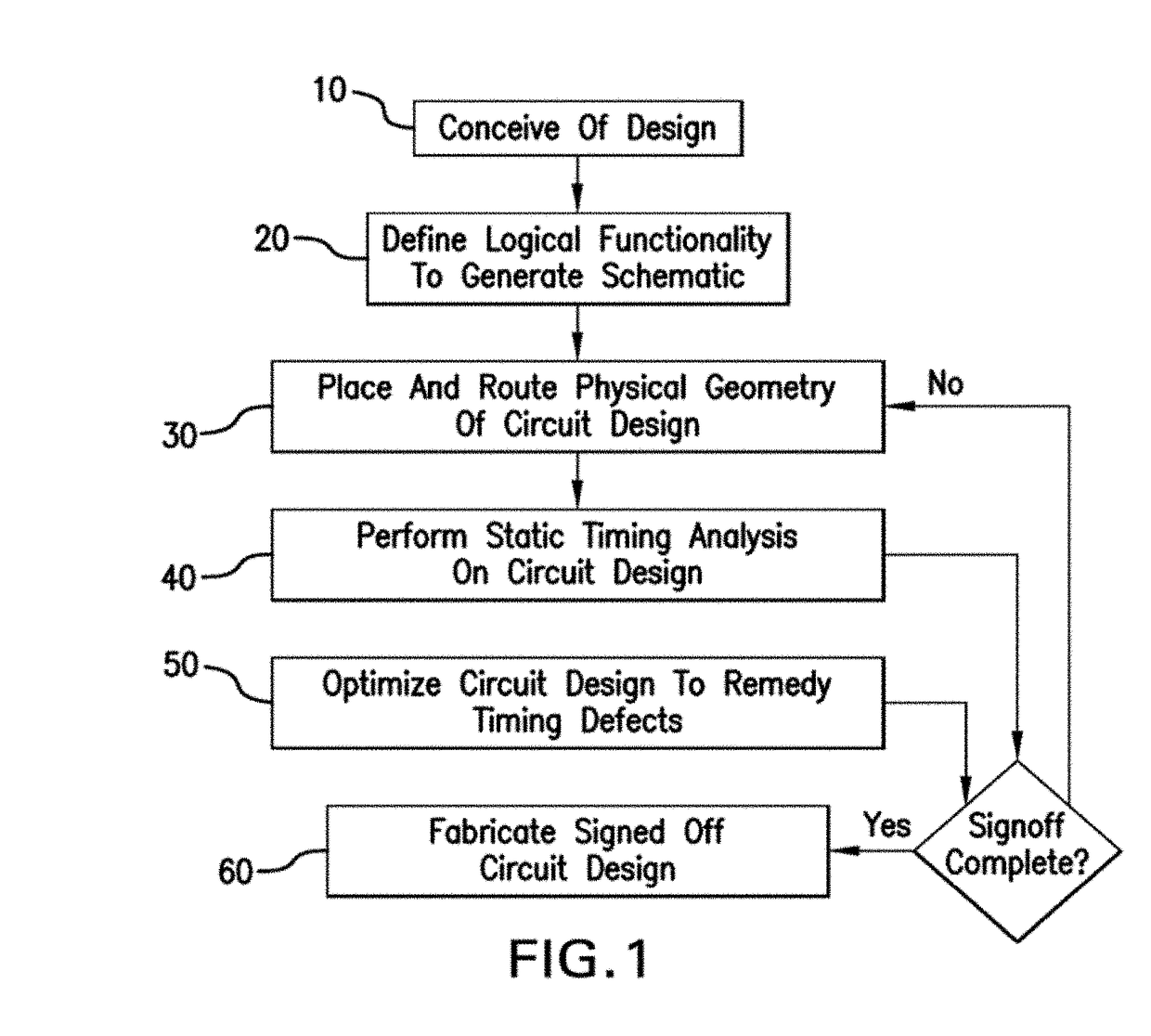
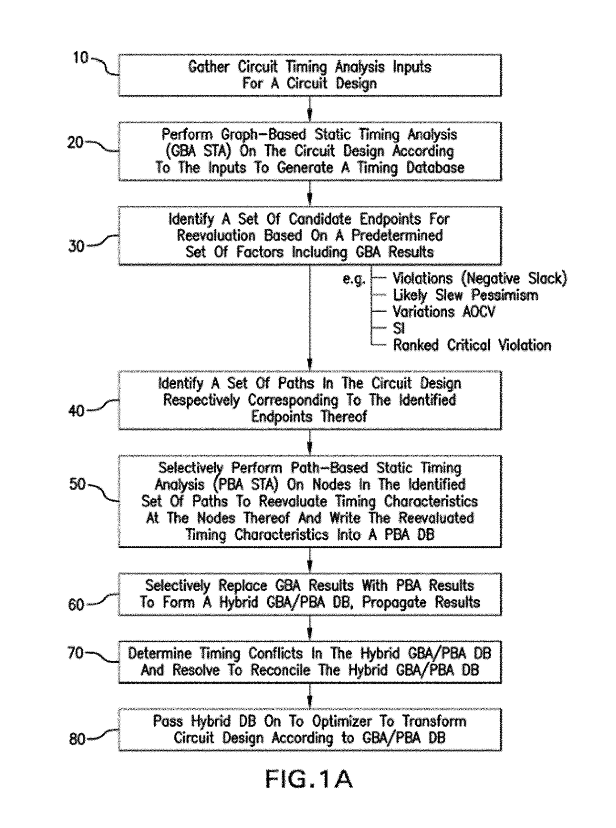
[0039]The subject system and method provide for guiding remedial transformations of a circuit design defined by physical implementation data to reduce needed physical corrections for detected violations in the circuit design. Such system and method execute with a goal of correlating timing between a physical implementation, corrective optimizer module, and a timing analysis module to reduce iterations and over or under correcting the circuit design therebetween.

[0040]A system and method formed in accordance wi...


PUM


Abstract

The present disclosure relates to a system and method for electronic design automation. Embodiments may include receiving, using at least one processor, an electronic design and determining one or more graph based analysis (“GBA”) violating nodes associated with the electronic design. Embodiments may include identifying a non-covered violating node from the GBA violating nodes and determining a worst timing path through the non-covered violating node. Embodiments may further include invoking a path-based analysis (“PBA”) on the worst timing path and determining if the worst timing path satisfies the PBA analysis.

Description

FIELD OF THE INVENTION[0001]The present disclosure relates to electronic design automation (EDA), and more specifically, to a method for performing path based analysis on an electronic design.DISCUSSION OF THE RELATED ART[0002]EDA utilizes software tools that may be used in the design and analysis of numerous electronic systems such as printed circuit boards (PCBs) and integrated circuits (ICs). Some EDA tools utilize static timing analysis as a method to assess the timing of any given digital circuit using software techniques and certain models that provide relevant characteristics of the digital circuit.[0003]While signoff systems and methods are known, such heretofore known systems and methods are encumbered by numerous deficiencies. Some of these include required repeated transformative iterations between timing signoff and physical implementation, highly divergent timing analysis between timing signoff and physical implementation optimizers—with highly pessimistic timing charac...

Claims


Application Information

Patent Timeline
Patent Type & Authority Patents(United States)
IPC IPC(8): G06F17/50
CPCG06F17/5081G06F17/5031G06F30/3312G06F30/398
Inventor VERMA, SOURABH KUMARKUMAR, NARESHTOMAR, AJAYAGARWAL, RAKESHGUPTA, UMESHBANSAL, MANISHGUHA, KAUSTAVSETHIA, PRASHANT
Owner CADENCE DESIGN SYST INC
Why Eureka
Try Eureka