Method, system, and computer program product for concurrent model aided electronic design automation

a technology of electronic design and computer program, applied in the field of method, system and computer program product of concurrent model aided electronic design automation, can solve the problems of time delay, insatisfactory solution, and certain wires being shorter at the expense of making other wires longer

Inactive Publication Date: 2008-07-03
CADENCE DESIGN SYST INC
View PDF49 Cites 44 Cited by
  • Summary
  • Abstract
  • Description
  • Claims
  • Application Information

AI Technical Summary

Problems solved by technology

However, making certain wires shorter usually comes at the expense of making other wires longer.
However, one problem exists for these methods.
Nonetheless, because larger gates also have larger capacitance and thus increases timing delay, the above solution does not satisfactorily solve the problems caused by increasingly shrinking feature sizes.
Another problem with using larger gates is that larger gates with larger drive strength tend to worsen the problem of electro-migration.
As a result of the momentum exchange, metal tends to deposit in the direction of the electron flow, and voids thus form at the grain boundaries and reduce the conductivity.
Such voids may over time cause the interconnect to stop conducting electricity altogether and thus cause the interconnect to fail.
As the devices shrink smaller, the delay caused by the increased R-C time constant becomes more significant over the delay caused by the actual wire length.
However, the use of low-k dielectric material aggravates the electro-migration problem due to the poor thermal conductivity of these low-k dielectric materials.
Although this assumption arose out of a practical consideration and has worked while the thickness variation is relatively insignificant as compared to the geometry sizes, such an assumption appears to be outdated, especially in light of the current development in incorporating the topological variations of each film into the electronic designs and the continuously shrinkage in sizes of device features.
Moreover, wire width cannot be arbitrarily changed due to the polycrystalline structure of the interconnect materials.
Nonetheless, the above rule-based methods pose new problems.
For instance, a good interconnect may be wrongfully determined to be improper for failing to meet the density rules or for producing unacceptable R-C delay even though the interconnect actually satisfies the design goals by having certain thickness that is different from the assumed value.
A contrary example is that a bad interconnect may also be wrongfully determined to be proper for meeting the metal density rules and / or the delay requirement.
The flaw in these two approaches, as interconnects get longer, is that wire resistance can no longer be neglected.
This is no longer true as the geometry continually shrinks, especially into the deep submicron technologies.
Other timing-driven placement methods may also be ineffective because they rely on the quality of the placement and the accuracy of the timing model.
Nonetheless, RET without taking the surface topology into consideration may pose further challenges to the timing closure due to the continual pursuit for smaller geometry size and the use of shorter wavelength on the lithographic tools such as the 193 nm λ ultra-high NA lithography or even the Extreme Ultra Violet lithography, especially in the deep submicron and increasing clock frequency designs.
However, larger NA also decreases the depth of focus, and such decreased depth of focus causes the lithographic tools' ability to print accurate circuits to be more sensitive to the topographical variation of the films on the wafer.
These foundry-imposed rules, however, do not take into account the types, functionality, performance specifications of the design; they are indeed manufacturing requirements primarily to ensure that the fabrication yield exceeds some economical number, and to allow the foundry to specify reasonably tight limits on electrical properties such as R and C per unit length.
However, in many cases these rules are un-necessarily strict.
Excessive power consumption of the IC inherently dissipates more heat which would cause the bonding or glue layer to deteriorate or ultimately fail.
Due to the continual effort to shrink the feature sizes and to package more features into a smaller die, the design closure problem has become much more complex.
Also, modern integrated circuits commonly operate at much higher frequencies, normally in the gigahertz range, which makes the integrated circuits more susceptible to noises such as cross-talk noise.
Moreover, smaller feature sizes normally cause negative effects on the electrical properties of various components in the integrated circuits and thus may adversely impact other aspects of the integrated circuit design.
In the previous example where there are too many timing constraint violations after routing, it may no longer economically feasible for the designer to go back and re-route the entire design because doing so would not only cause great delay in the entire design process and thus adversely impacts the time to market but may also incur substantial costs due to the large amount of computation required for such circuits.
This problem is further exacerbated due to the dilemma that typically the earlier a design constraint is addressed during a design flow, the more flexibility there will be to properly address the constraint, but the earlier one is in a design flow, the more difficult it is to predict the circuit's compliance with such constraints.

Method used


Image

  • Method, system, and computer program product for concurrent model aided electronic design automation
  • Method, system, and computer program product for concurrent model aided electronic design automation
  • Method, system, and computer program product for concurrent model aided electronic design automation

Examples


Embodiment Construction

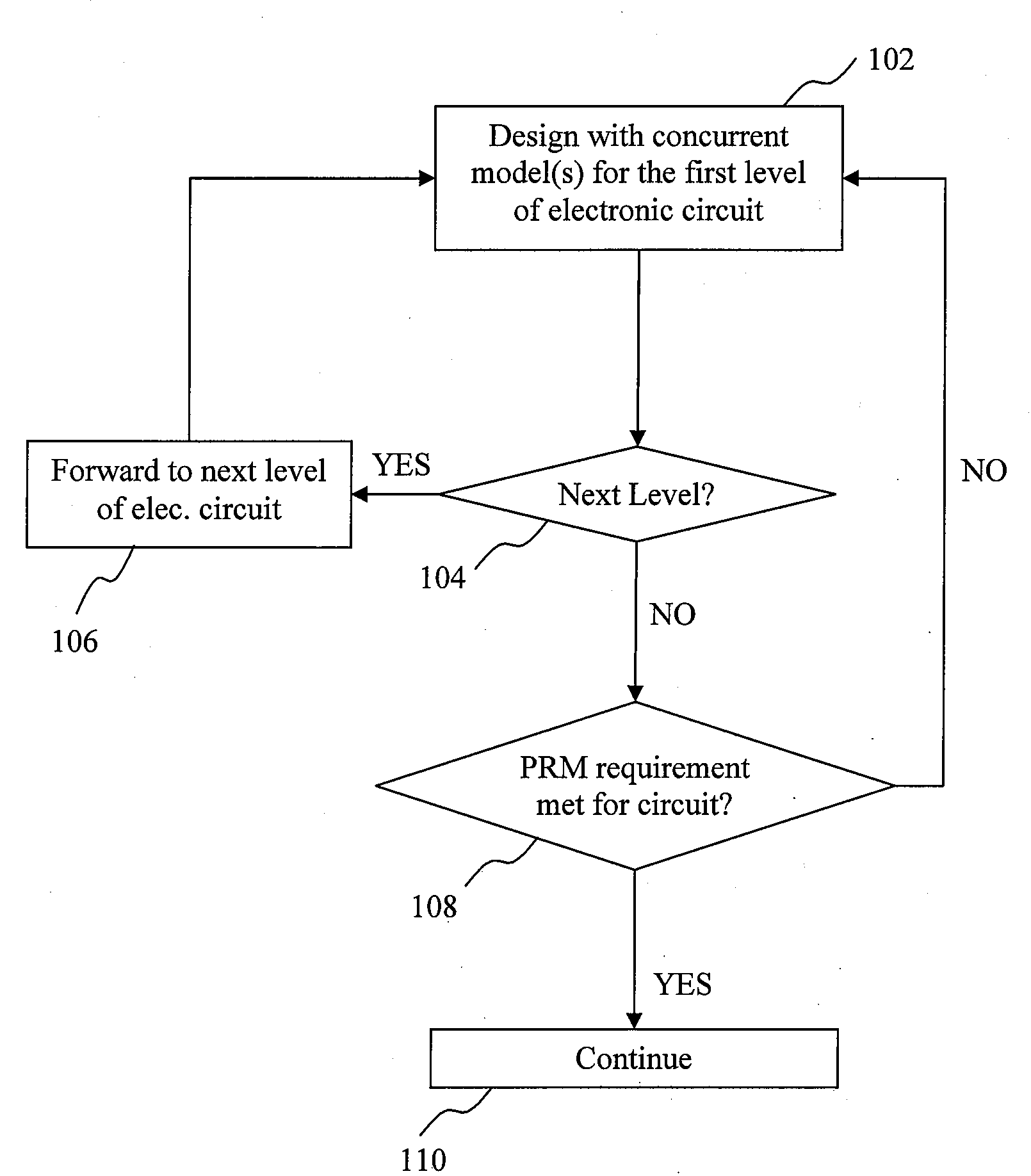
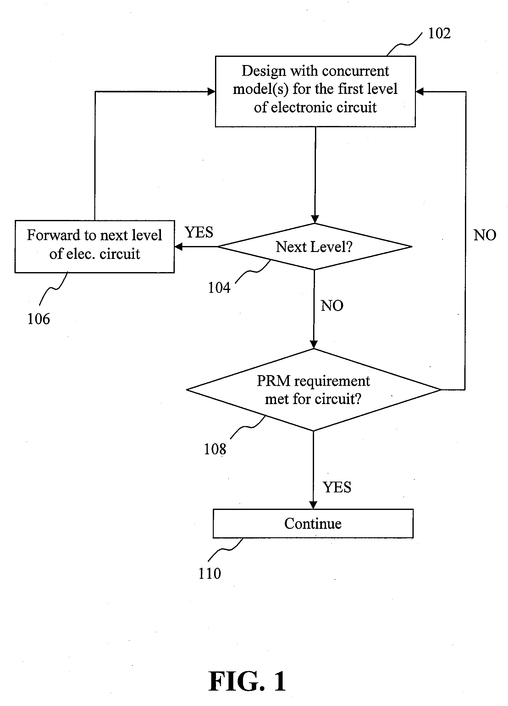
[0024]The present invention is directed to an improved method, system, and computer program product for designing an electronic circuit with concurrent models for fabrication, metrology, or image processing processes or techniques (e.g., RET). Some embodiments of the present invention utilize the above method, system, and / or computer program to produce more effective and accurate design closure for electronic circuit designs by evaluating the performance, manufacturability, or reliability (PMR) of the electronic circuit. The method or system of various embodiments of the present invention takes into consideration the geometric characteristics of one or more features of the electronic circuit to be manufactured or the impact of variation of surface topology of an underlying level and to more accurately and effectively estimate various metrics of the electronic circuit and thus more precisely predict or evaluate various objectives of the electronic circuit.

[0025]FIG. 1 depicts a high ...


PUM


Abstract

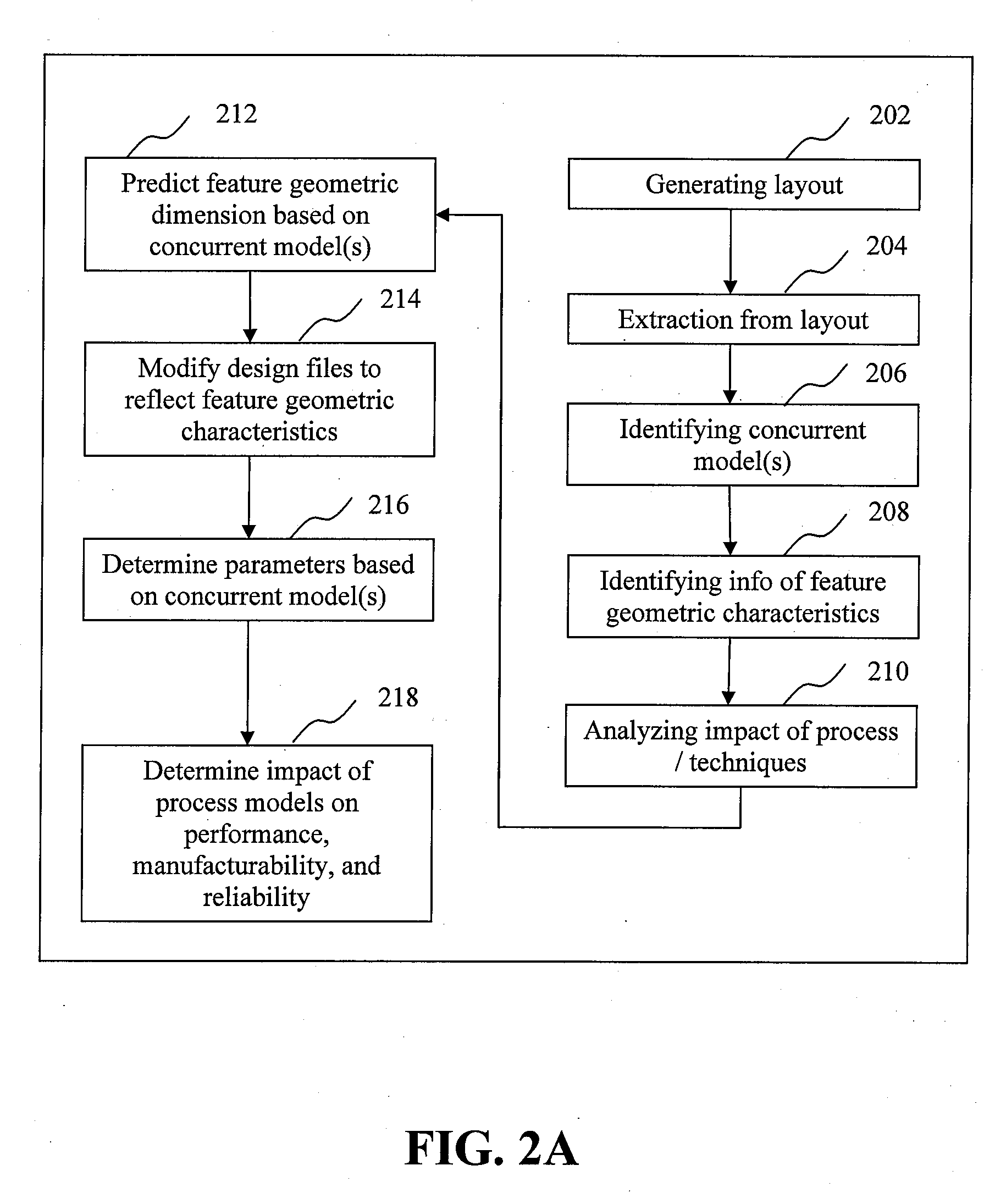
Disclosed are improved methods, systems, and computer program products for predicting performance, manufacturability, and reliability (PMR) using concurrent model analyses for electronic designs. Various embodiments of the present invention disclose a method for predicting PMR with concurrent process model analysis in which a method with concurrent model(s) generate a design for the one or more layers in the electronic circuit. The method then analyzes the impact of the processes or techniques for feature geometric characteristic predictions or PMR evaluations, based upon the concurrent models. Results may be reported to the users, or the method may modify the designs to accommodate the variations and determines one or more parameters based upon the concurrent models. One embodiment determines the impact of concurrent model on one or more of performance, manufacturability, and reliability criteria.

Description

CROSS-REFERENCE TO RELATED APPLICATION(S)[0001]This application claims the benefit of U.S. Provisional Application No. 60 / 877,870, filed on Dec. 29, 2006, which is hereby incorporated by reference in its entirety.BACKGROUND OF THE INVENTION[0002]As the electronic design feature size continues to shrink into deep submicron regime and the clock frequency increases, the electric properties of wires become more prominent, and chips are more susceptive to breakdown during fabrication due to, for example, antenna effect or to wear out over time due to, for example, electro-migration. Some prior methods propose prioritizing the nets and forcing shorter wire lengths among the high-priority, timing critical nets. However, making certain wires shorter usually comes at the expense of making other wires longer. Some other prior methods use larger gates with bigger transistors and higher drive strengths to charge the capacitance of wires more quickly and therefore making the path faster to maint...

Claims


Application Information

Patent Timeline
Patent Type & Authority Applications(United States)
IPC IPC(8): G06F17/50
CPCG03F7/70625G03F7/705
Inventor WHITE, DAVIDSCHEFFER, LOUIS K.
Owner CADENCE DESIGN SYST INC
Why Eureka
Try Eureka