Method, system, and computer program product for timing closure in electronic designs

a technology of electronic circuit design and timing closure, applied in the field of timing closure method, system and computer program product in electronic design, can solve the problems of complex semiconductor fabrication process, increasing difficulty in timing closure, and profound challenges in electronic circuit design

Active Publication Date: 2008-07-03
CADENCE DESIGN SYST INC
View PDF39 Cites 40 Cited by
  • Summary
  • Abstract
  • Description
  • Claims
  • Application Information

AI Technical Summary

Benefits of technology

[0011]As such, there exists a need for a more effective and accurate methodology for timing closure problems, especially in the deep submicron and increasing clock frequency designs. The present invention is directed to an improved method, system, and computer program product for performing timing closure for electronic designs. According to some embodiments of the present invention, the user may incorporate models for imaging processing techniques (such as RET), fabrication processes, or metrology processes to accurately predict the probability distribution of the performance of the electronic design in question.

Problems solved by technology

Timing closure has become increasingly difficult and presents some profound challenges in electronic circuit designs.
As device geometry shrinks, semiconductor fabrication processes require more complex techniques to meet the design goals such as lower power supply, thinner gate oxides, shorter channel length, higher body doping concentration, and thinner silicon films.
More importantly, the timing delay caused by the wires becomes more significant and can no longer be ignored.
As the device size continues to shrink and the clock frequency nevertheless increases, particularly into the deep-submicron regime, the electrical properties of wires or conductors become more prominent, and integrated circuit chips are more susceptible to breakdowns during fabrication due to, for example, the antenna effect or due to wear out or degradation over time due to, for example, electro-migration.
However, making certain wires shorter usually comes at the expense of making other wires longer.
However, there exists one problem for these methods.
Nonetheless, because larger gates also have larger capacitance and thus increases power and perhaps timing delay, the above method does not satisfactorily solve the problems caused by increasingly shrinking feature sizes. FIG. 1 illustrates a
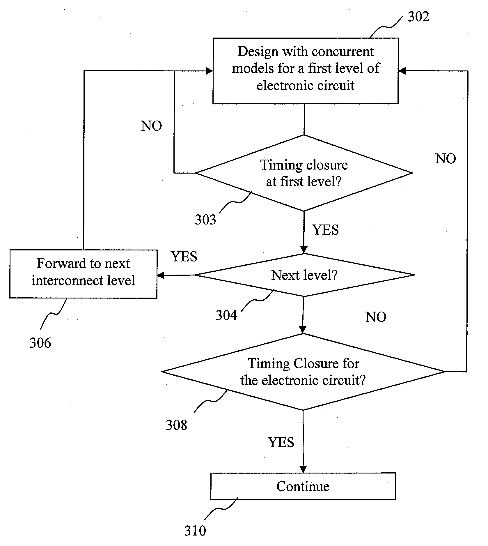
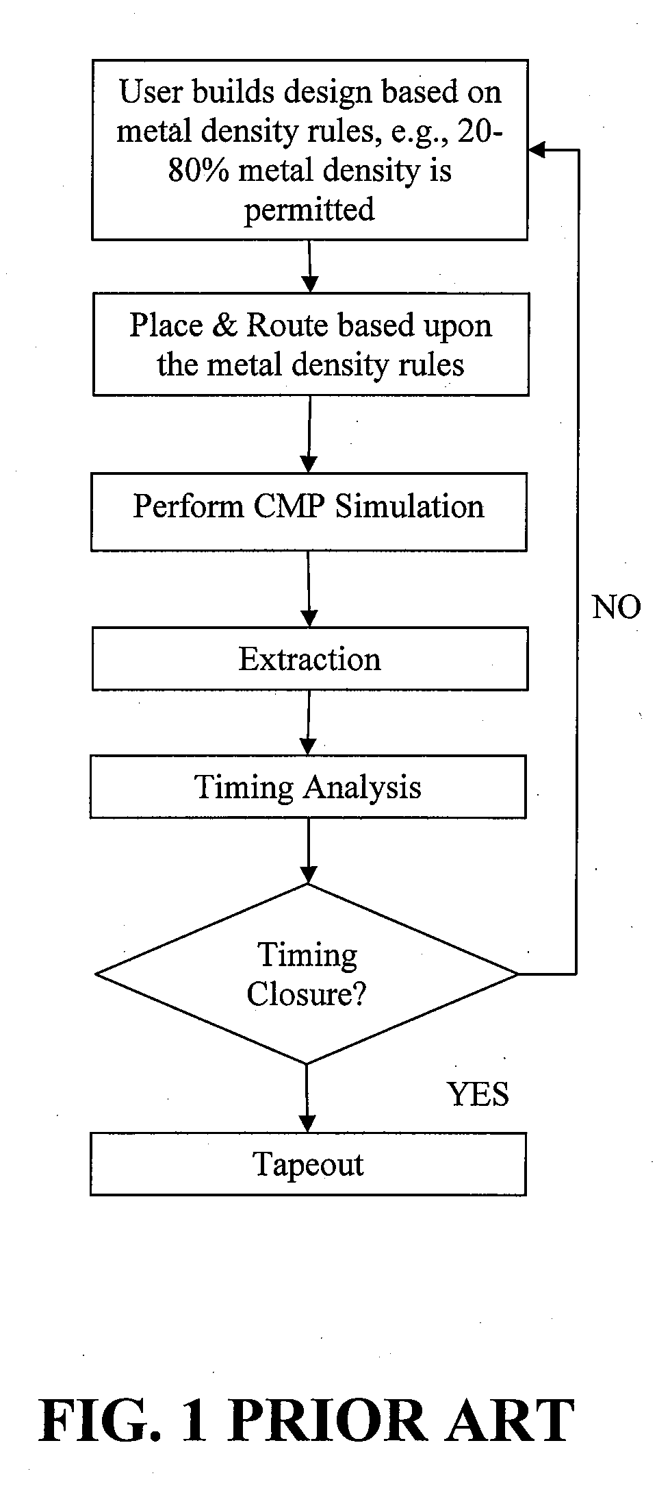
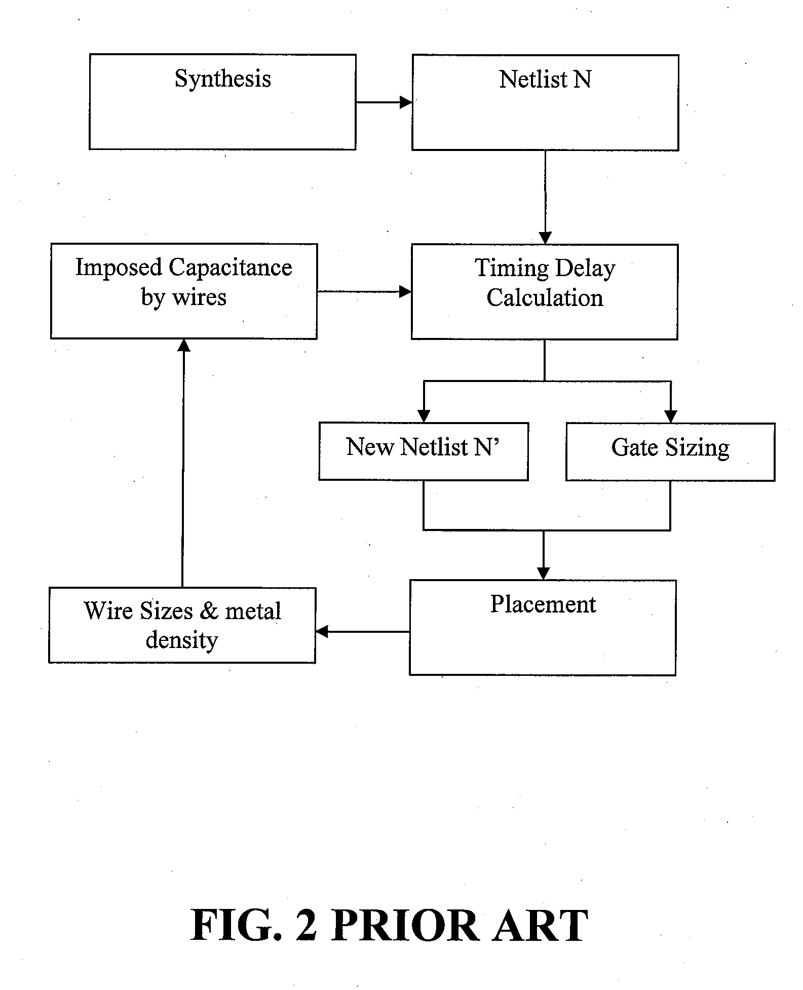
 general method of timing closure, and FIG. 2 illustrates a method of timing closure with gate sizing.
Another problem with using larger gates is that larger gates with larger drive strength tend to worsen the problem of electro-migration.
As a result of the momentum exchange, metal tends to deposit in the direction of the electron flow, and voids thus form at the grain boundaries and reduce the conductivity.
Such voids may over time cause the interconnect to stop conducting electricity altogether and thus cause the interconnect to fail.
As the devices shrinks to smaller sizes, the delay caused by the increased R-C time constant becomes more significant over the delay caused by the actual wire length.
However, the use of low-k dielectric material also aggravates the electro-migration problem due to the poor thermal conductivity of these low-k dielectric materials.
Although this assumption of constant wire thickness arose out of a practical consideration and has worked while the thickness variation is relatively insignificant as compared to the geometry sizes, such an assumption appears to be outdated, especially in light of the current development in incorporating the topological variations of each film into the electronic designs and the continuously shrinkage in sizes of device features.
Moreover, wire width cannot be arbitrarily altered due to the polycrystalline structure of the interconnect materials.
Nonetheless, the above rule-based methods pose new problems and challenges in electronic designs.
For instance, a good interconnect may be wrongfully determined to be improper for failing to meet the density rules or for producing unacceptable R-C delay even though the interconnect actually satisfies the design goals by having certain thickness that is different from the assumed value.
A contrary example is that a bad interconnect unfit for the design intent or goals may nonetheless be wrongfully determined to be proper for meeting the metal density rules and / or the delay requirement.
The flaw in these approaches, as interconnects get longer, is that wire resistance can no longer be neglected as it usually is in these gate sizing approaches.
This is no longer true as the geometry continually shrinks, especially into the deep submicron technologies.
Another approach by employing timing-driven placement methods may also be ineffective because these methods rely only on and are thus limited by the quality of the placement and the accuracy of the timing model.
Furthermore, one common limitation of all these approaches is that these approaches only change the placement and / or the nominal, center-line routing.
Nonetheless, applying these resolution enhancement techniques without taking the surface topology of certain features of the electronic design into consideration may pose further challenges to timing closure due to the continual pursuit for smaller geometry sizes and the use of shorter wavelengths on the lithographic tools such as the 193 nm λ ultra-high NA (numerical aperture) lithography or even the Extreme Ultra Violet lithography, especially in the deep submicron and increasing clock frequency designs.
However, larger NA also decreases the depth of focus, and such decreased depth of focus causes the lithographic tools' ability to print accurate circuits to be more sensitive to the topographical variation of the films on the wafer.

Method used


Image

  • Method, system, and computer program product for timing closure in electronic designs
  • Method, system, and computer program product for timing closure in electronic designs
  • Method, system, and computer program product for timing closure in electronic designs

Examples


Embodiment Construction

[0023]The present invention is directed to an improved method, system, and computer program product for an electronic design tool with concurrent models for fabrication, lithography, metrology, and / or imaging processing processes or techniques such as the resolution enhancement techniques (RET). Some embodiments of the present invention utilize the above method, system, and / or computer program to produce more effective and accurate performing timing closure for electronic design. As noted above, conventional methods and systems neglects the impact of variation of surface topology on the silicon and thus either use unnecessary computation resources to produce the results or even to produce unsatisfactory results. The proposed methodologies may be applied at least to the fields of placement, routing, trial route, global route, detailed route, and floorplanning.

[0024]Various embodiments of the invention may be implemented in numerous ways, including as software, hardware (e.g., an elec...


PUM


Abstract

Disclosed is an improved method, system, and computer program product for timing closure with concurrent models for fabrication, metrology, lithography, and / or imaging processing analyses for electronic designs. Some embodiments of the present invention disclose a method for timing closure with concurrent process model analysis in which a design tool with such concurrent models generates a design for the one or more interconnect levels. The method or system then analyzes the effects of the concurrent models to predict feature dimension variations based upon the concurrent models. The method or system then modifies the design files to reflect the variations and determines one or more parameters based upon the concurrent models. One embodiment then determines the impact of concurrent models upon the electrical and timing performance.

Description

CROSS-REFERENCE TO RELATED APPLICATION(S)[0001]This application claims the benefit of U.S. Provisional Application No. 60 / 878,008, filed on Dec. 29, 2006, which is hereby incorporated by reference in its entirety.BACKGROUND OF THE INVENTION[0002]Timing closure has become increasingly difficult and presents some profound challenges in electronic circuit designs. The main goal of computer-aided design simulations is obtaining desired device electrical characteristics. Nonetheless, geometric dimensions and profiles of features of an electronic circuit design often have significant impact on the device electrical characteristics. The device dimensions which may have significant impact on the electrical characteristics include, for example, gate oxide thickness, gate width and length, shape of the poly gate at the bottom, and spacer width. As device geometry shrinks, semiconductor fabrication processes require more complex techniques to meet the design goals such as lower power supply, t...

Claims


Application Information

Patent Timeline
Patent Type & Authority Applications(United States)
IPC IPC(8): G06F17/50
CPCG06F17/5009G06F2217/84G06F2217/12G06F17/5068G06F30/39G06F2119/18G06F2119/12G06F30/20Y02P90/02
Inventor SCHEFFER, LOUIS K.WHITE, DAVID
Owner CADENCE DESIGN SYST INC
Why Eureka
Try Eureka