Embedded electronic component and method of manufacturing electronic component embedded substrate

a technology of embedded substrates and electronic components, which is applied in the direction of printed resistor incorporation, printed circuit non-printed electric component association, printed element electric connection formation, etc., can solve the problems of reducing the reliability of connection in the process of forming via holes, and the process of electrically connecting the contact pads of the active element to an external device is becoming more difficult, so as to improve the reliability of connection with external wiring and improve the efficiency of the embedding process

Active Publication Date: 2018-02-13
SAMSUNG ELECTRO MECHANICS CO LTD
View PDF9 Cites 0 Cited by
  • Summary
  • Abstract
  • Description
  • Claims
  • Application Information

AI Technical Summary

Benefits of technology

[0010]The present invention has been invented in order to overcome the above-described problems and it is, therefore, an object of the present invention to provide an embedded electronic component, which can improve reliability of connection with external wiring and efficiency of an embedding process, and a method of manufacturing an electronic component embedded substrate.

Problems solved by technology

Further, there are continuous efforts to make electronic devices slim by embedding the electronic components in substrates.
Accordingly, since the area of the contact pad itself should be reduced and the interval between the contact pads also should be reduced, a process of electrically connecting the contact pads of the active element to an external device is becoming more difficult.
In addition, when the electronic component is embedded in the substrate, a via, which passes through an insulating layer, should be electrically connected to the contact pad, but as the area of the contact pad itself and the interval between the contact pads are reduced, there is a great reduction in the connection reliability in a process of forming a via-hole or in a process of plating a via by plating.

Method used


Image

  • Embedded electronic component and method of manufacturing electronic component embedded substrate
  • Embedded electronic component and method of manufacturing electronic component embedded substrate
  • Embedded electronic component and method of manufacturing electronic component embedded substrate

Examples


Embodiment Construction

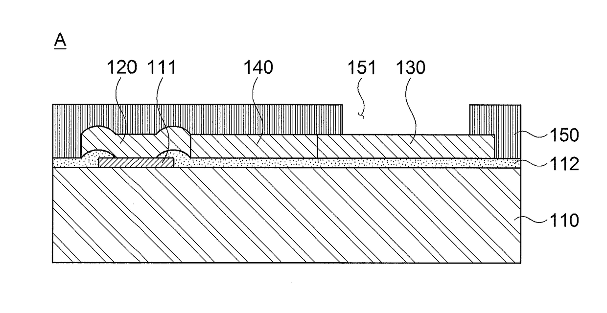
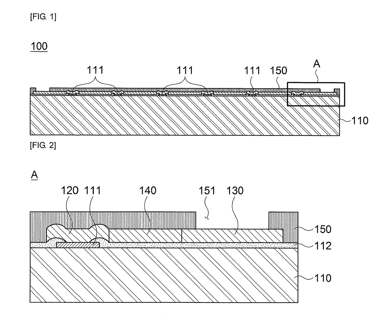
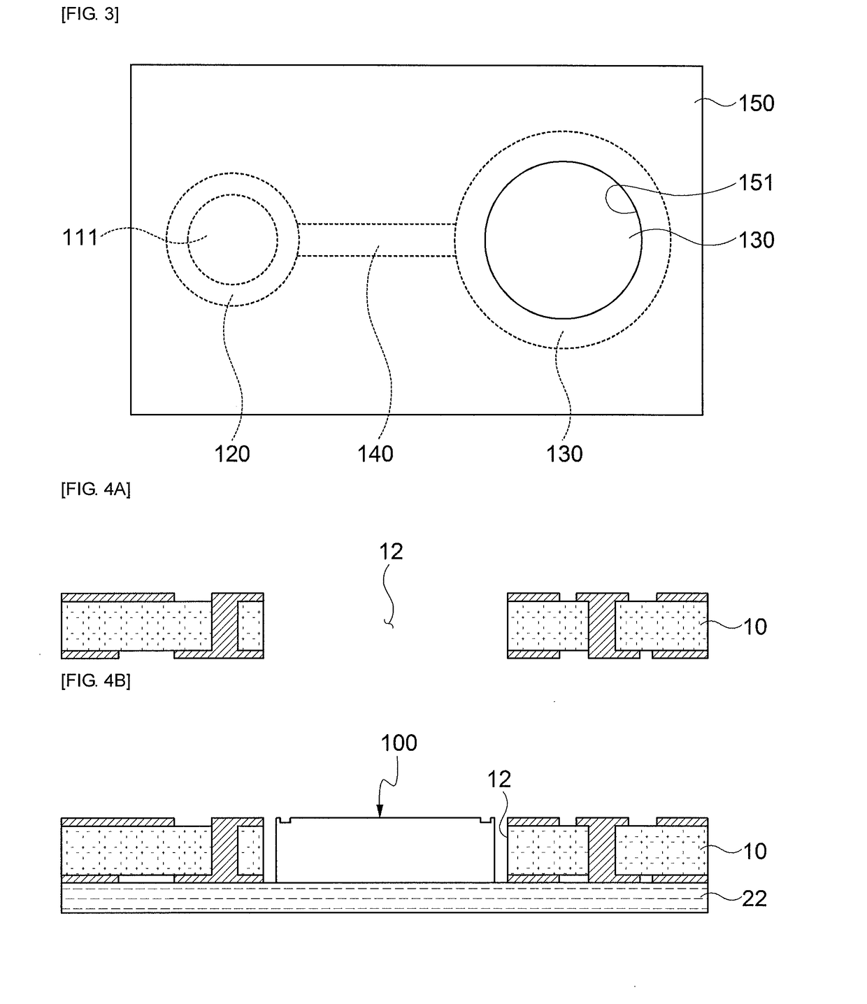
[0032]Advantages and features of the present invention and methods of accomplishing the same will be apparent by referring to embodiments described below in detail in connection with the accompanying drawings. However, the present invention is not limited to the embodiments disclosed below and may be implemented in various different forms. The embodiments are provided only for completing the disclosure of the present invention and for fully representing the scope of the present invention to those skilled in the art. Like reference numerals refer to like elements throughout the specification.

[0033]Terms used herein are provided to explain embodiments, not limiting the present invention. Throughout this specification, the singular form includes the plural form unless the context clearly indicates otherwise. When terms “comprises” and / or “comprising” used herein do not preclude existence and addition of another component, step, operation and / or device, in addition to the above-mentione...


PUM

PropertyMeasurementUnit
areaaaaaaaaaaa
thicknessaaaaaaaaaa
conductiveaaaaaaaaaa

Abstract

Disclosed is an embedded electronic component which can improve reliability of connection with external wiring and efficiency of an embedding process by including: a contact pad provided on at least one surface of a body portion and made of a conductive material; a first insulating layer for covering the at least one surface of the body portion; a first pad in contact with a surface of the contact pad and made of a conductive material; a rearrangement portion provided on a surface of the first insulating layer to be in contact with the first pad; a second pad provided on the surface of the first insulating layer to be in contact with the rearrangement portion; and a second insulating layer having an opening to expose a portion of the second pad while covering the first insulating layer, the first pad, the rearrangement portion, and the second pad.

Description

CROSS-REFERENCE TO RELATED APPLICATIONS[0001]This application claims the foreign priority benefit of Korean Patent Application Serial No. 10-2013-0096652 filed Aug. 14, 2013, which is hereby incorporated by reference in its entirety into this application.BACKGROUND OF THE INVENTION[0002]1. Field of the Invention[0003]The present invention relates to an embedded electronic component and a method of manufacturing an electronic component embedded substrate.[0004]2. Description of the Related Art[0005]Even though various electronic components such as passive elements and active elements are continuously becoming smaller, the functions of the electronic components are being further improved. Further, there are continuous efforts to make electronic devices slim by embedding the electronic components in substrates.[0006]Meanwhile, as the function and performance of the active elements such as IC chips are improved, the number of contact pads for electrically connecting external wiring and ...

Claims


Application Information

Patent Timeline
Patent Type & Authority Patents(United States)
IPC IPC(8): H05K1/18H05K7/10H05K7/12H01R9/00H05K1/16H05K1/11H05K3/40H01L21/56
CPCH05K1/185H01L21/568H01L2224/04105H05K1/114H05K1/162Y10T29/49146H05K1/167H05K3/4007H05K2201/10H05K2201/1003H05K2201/10022H05K1/165H05K3/46
Inventor LEE, DOO HWAN
Owner SAMSUNG ELECTRO MECHANICS CO LTD
Why Eureka
Try Eureka