Organic light emitting diode display

a light-emitting diode and organic technology, applied in the direction of basic electric elements, electrical equipment, semiconductor devices, etc., can solve the problems of deteriorated pixel and may not be corrected, and achieve the effect of preventing or reducing the light emitted from the pixel

Active Publication Date: 2018-04-03
SAMSUNG DISPLAY CO LTD
View PDF7 Cites 0 Cited by
  • Summary
  • Abstract
  • Description
  • Claims
  • Application Information

AI Technical Summary

Benefits of technology

[0027]According aspects of example embodiments of the present invention, it may be possible to prevent or reduce light emitted from the pixel from being extinguished while being transferred to the optical sensor unit.

Problems solved by technology

In OLED devices, however, the pixels may tend to deteriorate over time, and in order to improve or maintain image quality, OLED devices may correct or compensate for deterioration of the pixels.
However, if the light emitted from the pixel is transferred to the optical sensor unit, the deteriorated pixel may not be corrected.

Method used


Image

  • Organic light emitting diode display
  • Organic light emitting diode display
  • Organic light emitting diode display

Examples


Embodiment Construction

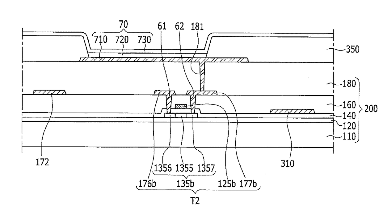
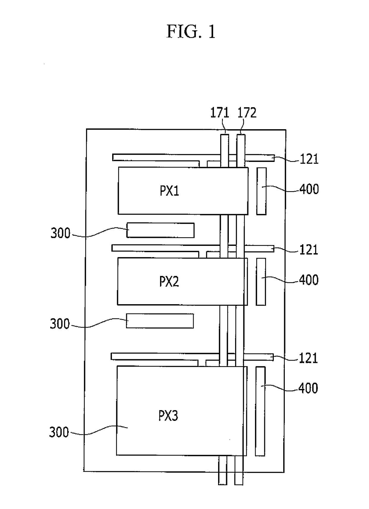
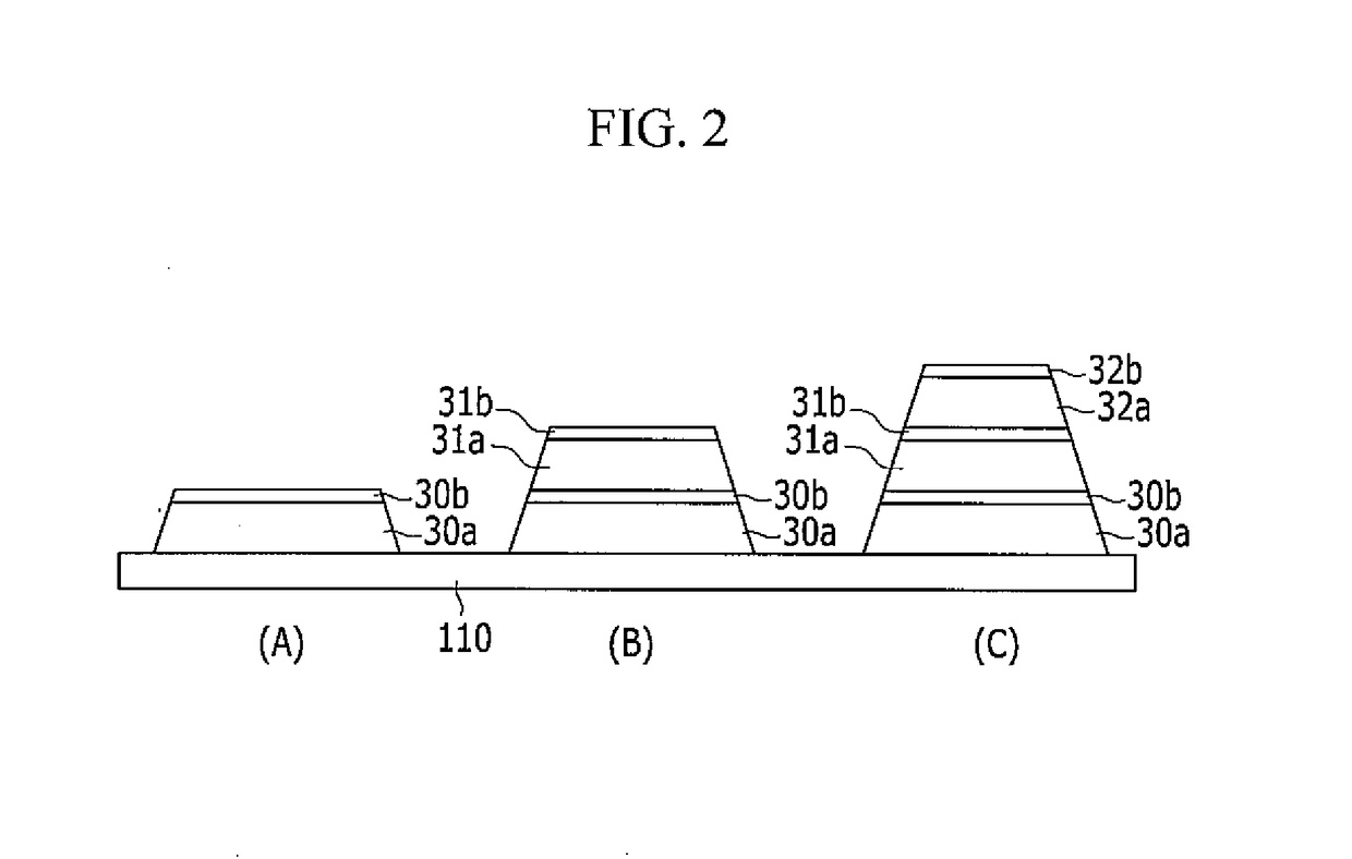
[0040]Hereinafter, example embodiments will be described in detail with reference to the accompanying drawings. As those skilled in the art would realize, the described embodiments may be modified in various different ways, all without departing from the spirit or scope of the present invention. On the contrary, example embodiments introduced herein are provided to make disclosed contents thorough and complete and sufficiently transfer the spirit to those skilled in the art.

[0041]In the drawings, the thickness of layers, films, panels, regions, etc., are exaggerated for clarity. It will be understood that when a layer is referred to as being “on” another layer or substrate, it can be directly on the other layer or substrate, or intervening them may also be present. Like reference numerals designate like elements throughout the specification.

[0042]It will be understood that when an element or layer is referred to as being “on,”“connected to,” or “coupled to” another element or layer,...


PUM


Abstract

An organic light emitting diode display includes: a substrate; a gate line on the substrate; a data line crossing the gate line; a driving voltage line extending parallel with at least one of the gate line and the data line; a first thin film transistor coupled to the gate line and the data line and comprising a first semiconductor layer; a second thin film transistor coupled to the first thin film transistor and the driving voltage line and comprising a second semiconductor layer; and an organic light emitting element coupled to the second thin film transistor, wherein at least one of the gate line, the data line, and the driving voltage line comprise a plurality of layers, and the lowest layer of the plurality of layers comprises a first metal layer made of a reflective metal.

Description

CROSS-REFERENCE TO RELATED APPLICATION[0001]This application claims priority to and the benefit of Korean Patent Application No. 10-2015-013812 filed in the Korean Intellectual Property Office on Jan. 28, 2015, the entire contents of which are incorporated herein by reference.BACKGROUND[0002]1. Field[0003]Aspects of embodiments of the present invention relate to an organic light emitting diode display.[0004]2. Description of the Related Art[0005]Display devices include, for example, a liquid crystal display (LCD), a plasma display panel (PDP), an organic light emitting diode device (OLED device), a field effect display (FED), an electrophoretic display device, and the like.[0006]OLED devices includes two electrodes and an organic emission layer positioned therebetween and emit light while an electron injected from one electrode and a hole injected from the other electrode are coupled with each other in the organic emission layer to form an exciton and the exciton discharges energy.[...

Claims


Application Information

Patent Timeline
Patent Type & Authority Patents(United States)
IPC IPC(8): H01L29/08H01L51/52H01L27/32
CPCH01L51/5271H01L27/3276H01L27/3269H10K59/13H10K59/131H10K59/878H10K50/856
Inventor KIM, BYOUNG KIKIM, HEE KYUNGSEO, IL HUNSHIN, YOUNG JUNCHUNG, YUN-MO
Owner SAMSUNG DISPLAY CO LTD
Why Eureka
Try Eureka