High frequency power supply device

a power supply device and high frequency technology, applied in the direction of dc-dc conversion, power conversion systems, climate sustainability, etc., can solve the problems of unbalanced voltage across the first capacitor, unsatisfactory zero voltage switching operation, and harmonic wave noise, so as to reduce the current capacity of the diode, reduce the emission of harmonic wave noise, and reduce the effect of harmonic wave components of the curren

Active Publication Date: 2021-05-18
MURATA MFG CO LTD
View PDF12 Cites 0 Cited by
  • Summary
  • Abstract
  • Description
  • Claims
  • Application Information

AI Technical Summary

Benefits of technology

[0007]Thus, the present disclosure provides a high frequency power supply device that reduces harmonic wave components contained in a current waveform of high frequency power output from a switching circuit and thus prevents or reduces emission of harmonic wave noise. Furthermore, another object of the present disclosure is to provide a high frequency power supply device that is capable of reducing harmonic wave components contained in the current waveform of high frequency power output from the switching circuit and thus preventing or reducing emission of harmonic wave noise both in the case where an operation for reducing switching loss is achieved by attaining a zero voltage switching (soft switching) operation and in the case where a non-zero voltage switching operation (hard switching) is performed instead of attaining the zero voltage switching (soft switching) operation.
[0023]According to the present disclosure, a high frequency power supply device in which harmonic wave components contained in a current waveform of high frequency power output from a switching circuit can be reduced and emission of harmonic wave noise can thus be reduced, can be obtained.

Problems solved by technology

However, there is a problem of harmonic wave noise caused by harmonic wave components contained in the current waveform being emitted from the coil or the antenna.
With the above configuration, a problem in which in the case where the impedance of the first impedance element and the impedance of the second impedance element are different, adverse influence of the difference between the impedances makes the ratio of time during which the voltage across the first capacitor changes and the ratio of time during which the voltage across the second capacitor changes unbalanced, can be solved.
Furthermore, in the case of leading of a current, a zero voltage switching operation is not attained.

Method used


Image

  • High frequency power supply device
  • High frequency power supply device
  • High frequency power supply device

Examples


first embodiment

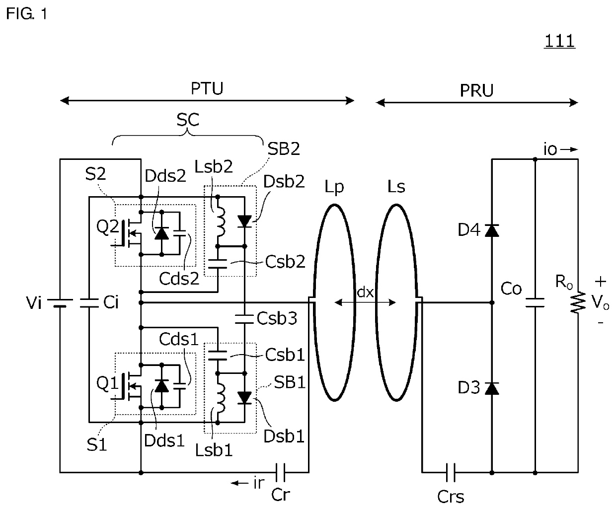
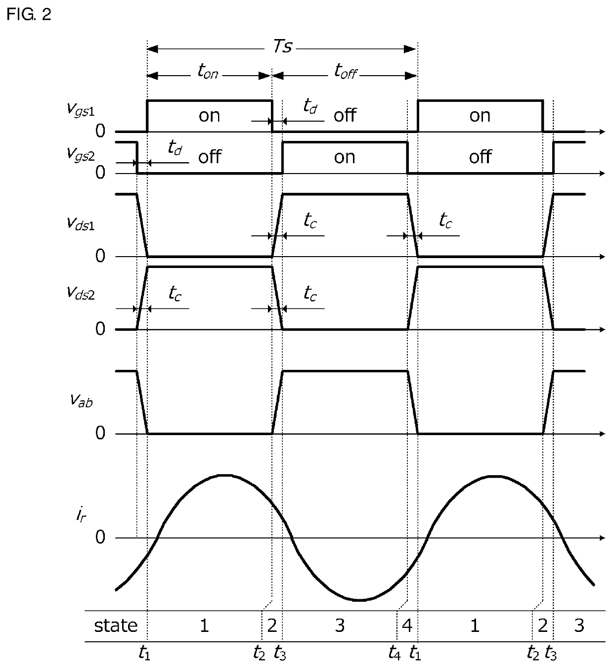
[0037]FIG. 1 is a circuit diagram of a power transfer system that includes a high frequency power supply device according to a first embodiment of the present disclosure.

[0038]A power transfer system 111 includes a power transmission device PTU and a power reception device PRU. The power transmission device PTU is an example of a “high frequency power supply device” according to the present disclosure.

[0039]The power transfer system 111 is a system that causes the power transmission device PTU to supply stable DC energy to the power reception device PRU.

[0040]The power transmission device PTU includes a DC power supply Vi, a switching circuit SC that is connected to an output side of the DC power supply Vi and generates high frequency power, a snubber circuit SB1 that is connected between both ends of a low-side switch circuit S1 included in the switching circuit SC, and a snubber circuit SB2 that is connected between both ends of a high-side switch circuit S2. The switching circuit...

second embodiment

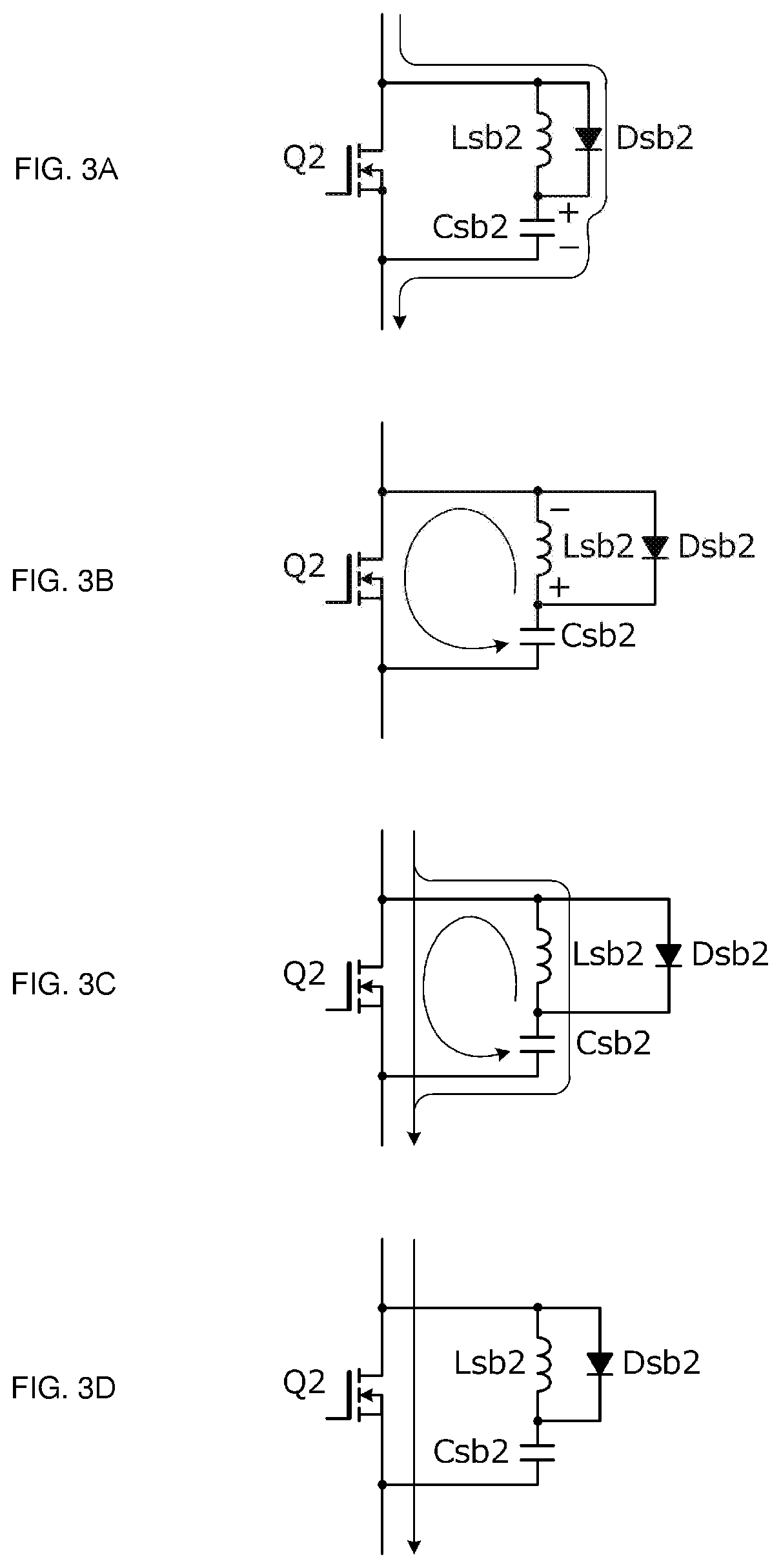
[0078]In a second embodiment, a high frequency power supply device in which a configuration of a snubber circuit is different from that in the first embodiment will be described.

[0079]FIG. 5 is a circuit diagram of a power transfer system 121 that includes the high frequency power supply device according to the second embodiment. The power transfer system 121 is different from the power transfer system 111 illustrated in FIG. 1 in a configuration of, in particular, a snubber circuit of the switching circuit SC of the power transmission device PTU.

[0080]In FIG. 5, the snubber circuit SB1 that is connected between both ends of the low-side switch circuit S1 and the snubber circuit SB2 that is connected between both ends of the high-side switch circuit S2 are provided.

[0081]The snubber circuit SB1 includes a series circuit including the inductor Lsb1 and the first capacitor Csb1. In a similar manner, the snubber circuit SB2 includes a series circuit including the inductor Lsb2 and the ...

third embodiment

[0084]In a third embodiment, a high frequency power supply device in which a configuration of a snubber circuit is different from that in the first and second embodiments will be described.

[0085]FIG. 7 is a circuit diagram of a power transfer system 131 that includes the high frequency power supply device according to the third embodiment.

[0086]In FIG. 7, the snubber circuit SB1 that is connected between both ends of the low-side switch circuit S1 and the snubber circuit SB2 that is connected between both ends of the high-side switch circuit S2 are provided.

[0087]The snubber circuit SB1 includes a series circuit including the inductor Lsb1 and the first capacitor Csb1 and the diode Dsb1 that is connected in parallel with the inductor Lsb1. In a similar manner, the snubber circuit SB2 includes a series circuit including the inductor Lsb2 and the second capacitor Csb2 and the diode Dsb2 that is connected in parallel with the inductor Lsb2. The power transfer system 131 is different fr...


PUM


Abstract

A switching circuit is connected to an output side of a DC power supply, includes a low-side switch circuit and a high-side switch circuit, and generates high frequency power by switching of the low-side switch circuit and the high-side switch circuit. Snubber circuits are connected between both ends of the low-side switch circuit and both ends of the high-side switch circuit. The snubber circuits include series circuits including inductors and capacitors, and include diodes that are connected in parallel with the inductors.

Description

CROSS-REFERENCE TO RELATED APPLICATIONS[0001]This application claims benefit of priority to International Patent Application No. PCT / JP2018 / 023278, filed Jun. 19, 2018, and to Japanese Patent Application No. 2017-134284, filed Jul. 10, 2017, the entire contents of each are incorporated herein by reference.BACKGROUNDTechnical Field[0002]The present disclosure relates to a high frequency power supply device that includes a high frequency power generation circuit connected to a DC power supply and generating high frequency power using a switching circuit allowing a switch element to be switched at a high frequency.Background Art[0003]A power supply device that is connected to a DC power supply, converts the DC power supply into high frequency power by switching of a switch element, and supplies power via the high frequency power is used for, for example, a wireless power transfer system.[0004]For example, in WO 2012 / 101907, a configuration that includes a high frequency power generatio...

Claims


Application Information

Patent Timeline
Patent Type & Authority Patents(United States)
IPC IPC(8): H02J50/12H02M1/34H02M1/00
CPCH02J50/12H02M1/34H02M2001/0058Y02B70/10H02M1/346H02M3/33571H02M3/33573H02M3/01H02M1/0058
Inventor HOSOTANI, TATSUYA
Owner MURATA MFG CO LTD
Why Eureka
Try Eureka