Array substrate, in-cell touch screen and touch display device

a touch display device and substrate technology, applied in the field of array substrates, can solve the problems of reducing the signal to noise ratio of the in-cell touch screen, increasing the thickness and weight of the entire display device, etc., and achieves the effects of enhancing the emission intensity of a touch signal, prolonging the boundary, and increasing the mutual capacitance between the sensing sub-electrode and the driving sub-electrod

Active Publication Date: 2018-04-17
BOE TECH GRP CO LTD +1
View PDF36 Cites 2 Cited by
  • Summary
  • Abstract
  • Description
  • Claims
  • Application Information

AI Technical Summary

Benefits of technology

[0020]According to the array substrate provided in the embodiments of the invention, the common electrode layer is divided into driving electrodes and sensing electrodes by altering an existing structure of the common electrode layer, and concave-convex structure in a staggered arrangement are formed at borders of adjacent driving sub-electrodes and sensing sub-electrodes to form a mutual nest structure, so as to achieve the purpose of prolonging boundaries between the driving sub-electrodes and the sensing sub-electrodes. Thus, mutual capacitance between the sensing sub-electrodes and the driving sub-electrodes is increased, emission intensity of a touch signal is enhanced, signal to noise ratio of the touch signal is increased, and therefore touch sensitivity is improved.

Problems solved by technology

The on-cell touch screen inevitably increases thickness and weight of the entire display device, thereby reducing light transmittance, which cannot meet requirement of the current development trend on a lighter and thinner display device.
However, compared with the on-cell touch screen, the in-cell touch screen has an unsolved technical difficulty that an electrode layer located inside a display panel is closer to a touch screen electrode, which is easy to cause interference between a touch signal and a display signal, thereby leading to a lower signal to noise ratio of the in-cell touch screen.

Method used


Image

  • Array substrate, in-cell touch screen and touch display device
  • Array substrate, in-cell touch screen and touch display device
  • Array substrate, in-cell touch screen and touch display device

Examples


first embodiment

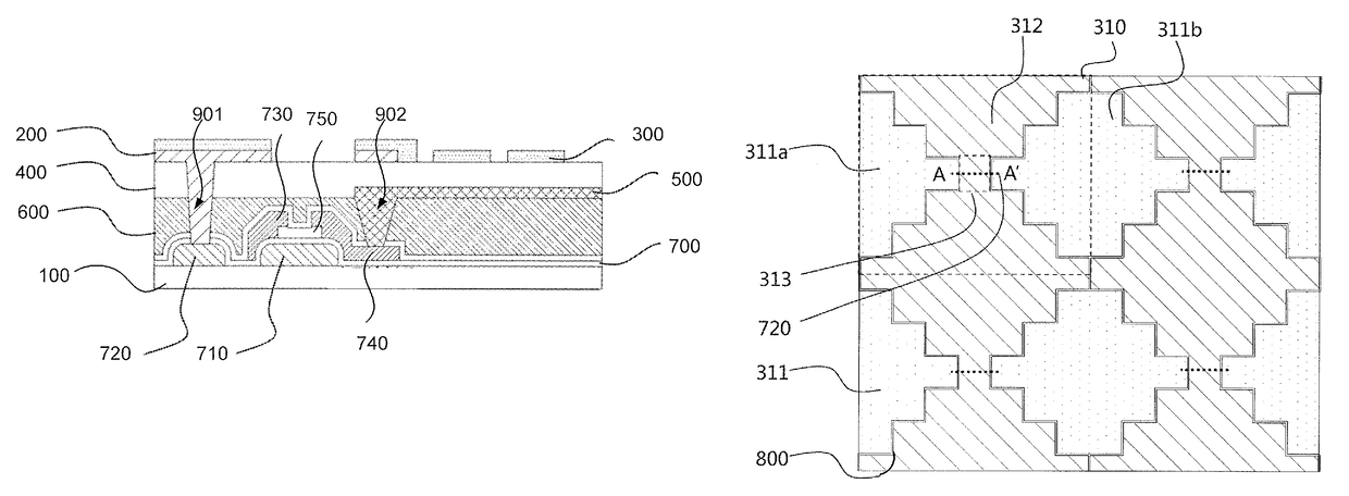
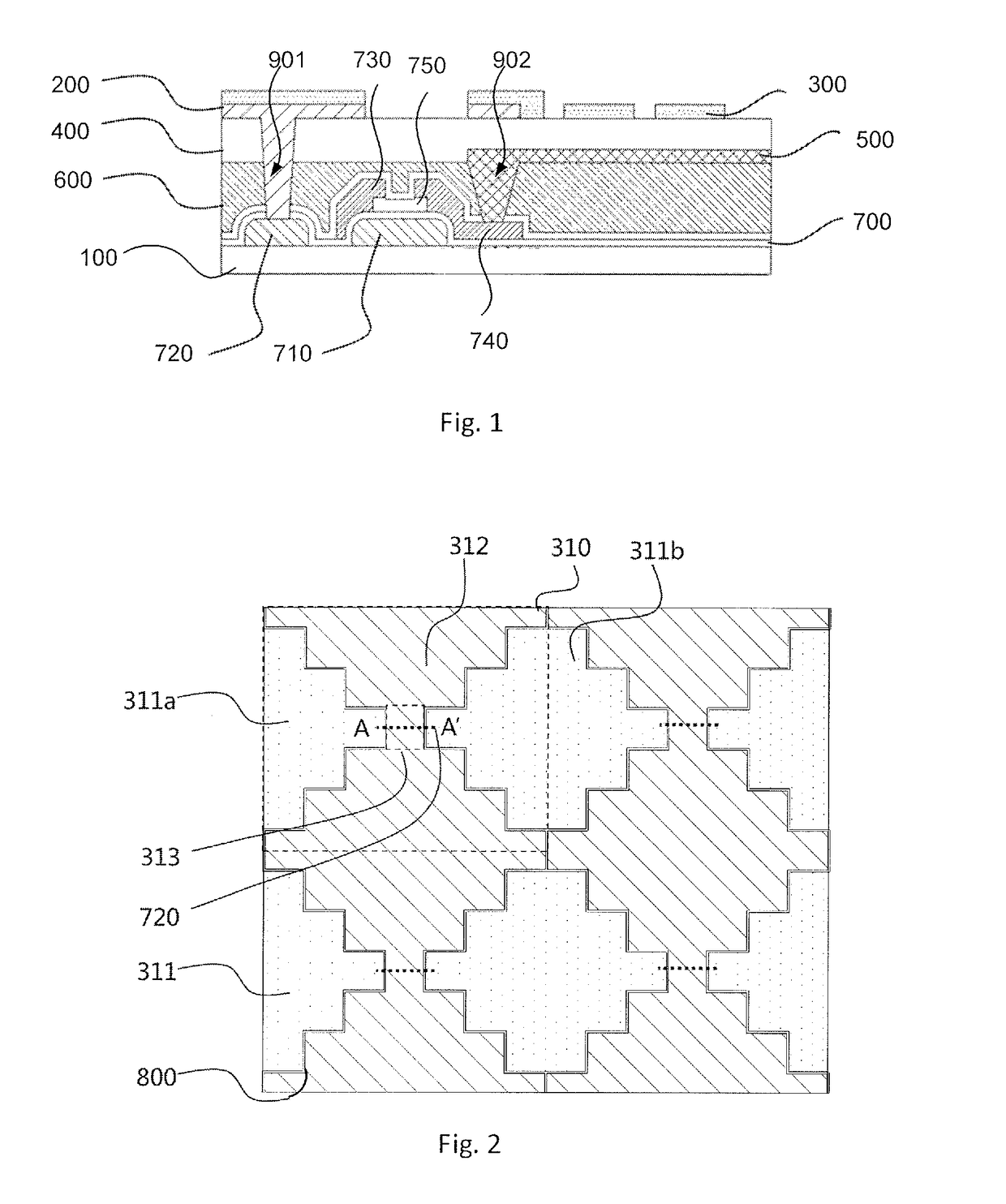
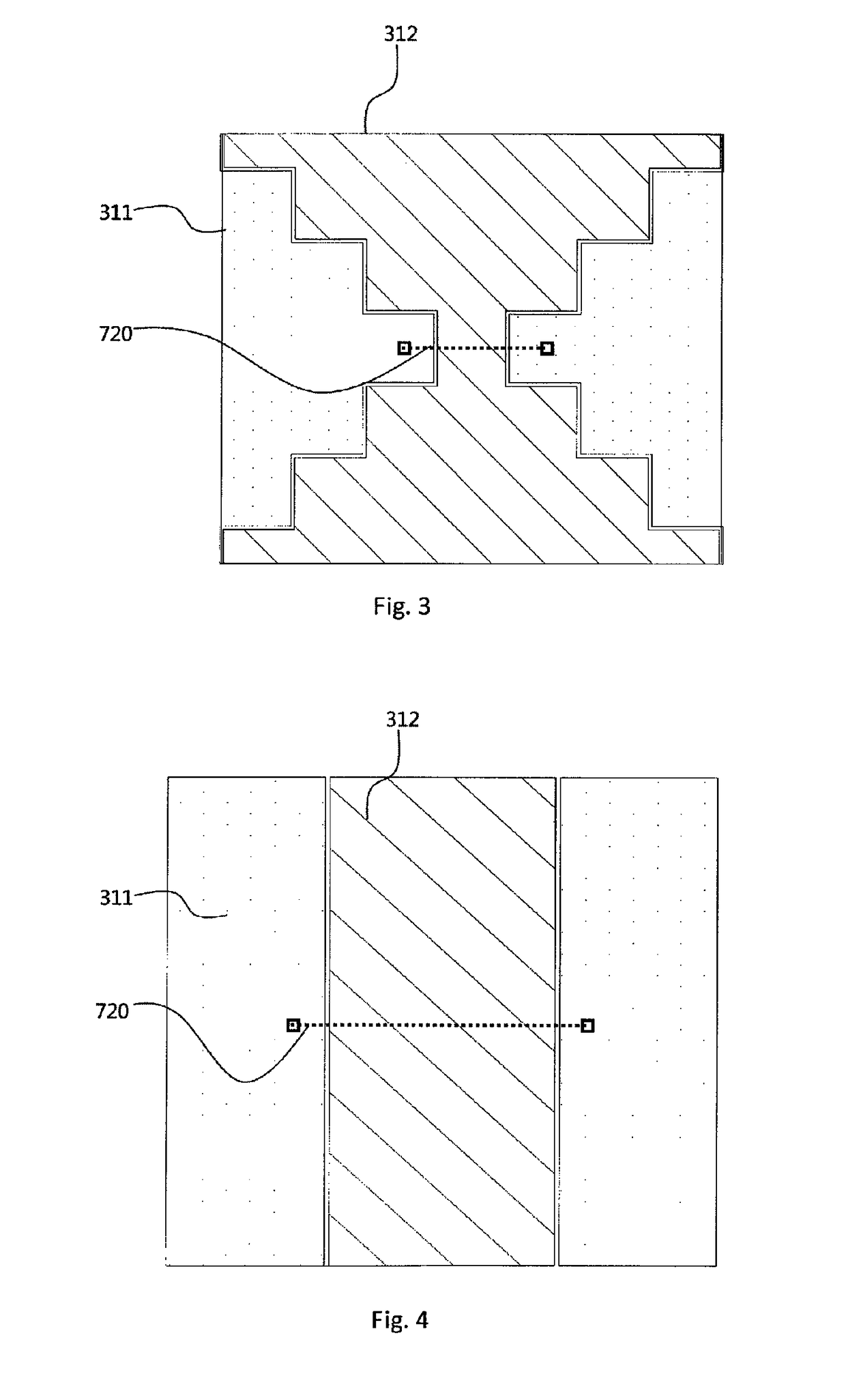
[0032]The embodiment of the invention provides an array substrate as illustrated in FIG. 1. The array substrate comprises a base substrate 100, and a gate electrode 710, a source electrode 730, a drain electrode 740 and a semiconductor layer 750 arranged on the base substrate 100, and further comprises a common electrode layer 300. The common electrode layer 300 is provided with a plurality of driving electrodes and a plurality of sensing electrodes with extending directions perpendicular to each other, wherein each of the driving electrodes includes a plurality of driving sub-electrodes which are connected to one another, each of the sensing electrodes includes a plurality of sensing sub-electrodes which are connected to one another, and adjacent driving sub-electrodes and sensing sub-electrodes have concave-convex structures in a staggered arrangement at borders and insulated from each other.

[0033]For example, the driving sub-electrode and the sensing sub-electrode have serrated e...

second embodiment

[0057]The second embodiment of the invention provides an in-cell touch screen, as illustrated in FIG. 7. The in-cell touch screen comprises a color filter substrate and the array substrate according to the first embodiment, wherein a black matrix 110 is further arranged between adjacent sub-pixel units on the color filter substrate, the driving metal wires 210, the sensing metal wires 220 as well as the borders 800 between the driving sub-electrodes 311 and the sensing sub-electrodes 312 are all corresponding to the black matrix in position, as illustrated in FIG. 8.

[0058]Therein, the color filter substrate comprises a base substrate 100, a black matrix 110 and a color filter layer 120, and it can be seen from FIG. 8 that the black matrix 110 on the color filter substrate can be corresponding to the border 800 between the a driving sub-electrode and an sensing sub-electrode on the array substrate, and can also be corresponding to a thin film transistor on the array substrate in posi...

third embodiment

[0059]The third embodiment of the invention further provides a touch display device, comprising the in-cell touch screen according to the second embodiment, which increases signal to noise ratio while realizing a touch and display function.

[0060]The touch display device provided in this embodiment may be electronic paper, a cell phone, a tablet computer, a TV set, a laptop, a digital photo frame, a navigator or any product or component with a display function.


PUM

PropertyMeasurementUnit
dielectric constantaaaaaaaaaa
included angleaaaaaaaaaa
dielectric constantaaaaaaaaaa

Abstract

An array substrate, an in-cell touch screen and a touch display device are provided. The array substrate includes a common electrode layer, wherein the common electrode layer is provided with a plurality of driving electrodes and a plurality of sensing electrodes with extending directions perpendicular to each other, each of the driving electrodes includes a plurality of driving sub-electrodes which are connected to one another, each of the sensing electrodes includes a plurality of sensing sub-electrodes which are connected to one another, and adjacent driving sub-electrode and sensing sub-electrode have concave-convex structures in a staggered arrangement at an border and are insulated from each other.

Description

TECHNICAL FIELD[0001]Embodiments of the invention relate to an array substrate, an in-cell touch screen and a touch display device.BACKGROUND[0002]On account of advantages such as accurate and sensitive positioning, good touch feeling, and long service life and the like, capacitive touch screens are more and more popular among manufacturers and users and are applied in many fields. The capacitive touch screens are divided into two types of self-capacitive touch screens and mutual-capacitive touch screens. Due to capability of multi-point touch, the mutual-capacitive touch screens become a mainstream and a future development trend in a capacitive touch screen market.[0003]The mutual-capacitive touch screens are divided into two structures, i.e., an on cell type and an in cell type. In an on-cell mutual-capacitive touch screen (hereinafter referred to as on-cell touch screen), a touch component is attached to an external part of a display panel, specifically to an external part of a c...

Claims


Application Information

Patent Timeline
Patent Type & Authority Patents(United States)
IPC IPC(8): G06F3/044G02F1/1343G06F3/041
CPCG06F3/044G06F3/0418G06F3/0412G02F1/134336G02F1/13338G06F3/0446G06F3/0443G02F1/134372
Inventor JIANG, RIKUN
Owner BOE TECH GRP CO LTD
Why Eureka
Try Eureka