Charge-trap layer separation and word-line isolation for enhanced 3-D NAND structure

a nand structure and charge-trap layer technology, applied in the field of semiconductor substrate processing, can solve the problems of leaking of trapped charges in such memory cells, increasing the aspect ratio of memory cell strings, and difficulty in maintaining memory hole uniformity and minimizing variation in memory cell dimensions

Active Publication Date: 2018-05-01
APPLIED MATERIALS INC
View PDF3 Cites 98 Cited by
  • Summary
  • Abstract
  • Description
  • Claims
  • Application Information

AI Technical Summary

Problems solved by technology

As the number of vertically stacked memory cells in 3D NAND devices increases, the aspect ratio of memory cell strings also increases, introducing numerous manufacturing issues, including difficulty in maintaining memory hole uniformity and minimizing variation in memory cell dimensions.
However, with thinner insulator layers, memory cells in a NAND string are more closely spaced, and leakage of trapped charges in such memory cells may occur, compromising stored data or bits.
In addition, when memory cells are more closely spaced, fringing effects caused by the rectangular cross-section of a memory cell can further affect charge stored in neighboring memory cells.

Method used


Image

  • Charge-trap layer separation and word-line isolation for enhanced 3-D NAND structure
  • Charge-trap layer separation and word-line isolation for enhanced 3-D NAND structure
  • Charge-trap layer separation and word-line isolation for enhanced 3-D NAND structure

Examples


Embodiment Construction

[0018]In the following description, numerous specific details are set forth to provide a more thorough understanding of the embodiments of the present disclosure. However, it will be apparent to one of skill in the art that one or more of the embodiments of the present disclosure may be practiced without one or more of these specific details. In other instances, well-known features have not been described in order to avoid obscuring one or more of the embodiments of the present disclosure.

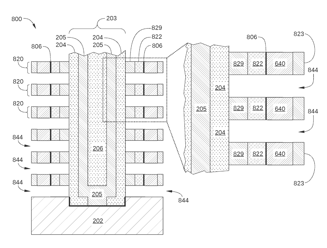
[0019]In a conventional three-dimensional (3D) NAND memory device, the charge storage region of a memory cell may be susceptible to leakage of trapped charge into or out of the charge storage region of adjacent memory cells, compromising stored data, as illustrated in FIG. 1. FIG. 1 is a schematic cross-sectional view of a portion 150 of a conventional three-dimensional (3D) NAND memory device 100. Portion 150 includes memory cells 131, 132, and 133, each separated by insulator layers 110, such as ...


PUM


Abstract

In a 3D NAND device, the charge trap region of a memory cell is formed as a separate charge-trap “island.” As a result, the charge-trap region of one memory cell is electrically isolated from charge-trap regions in adjacent memory cells. The charge trap region of one memory cell is separated from the charge trap regions of adjacent memory cells by a dielectric structure, such as a silicon oxide film. Alternatively, the charge trap region of a memory cell is separated from the charge trap regions of adjacent memory cells by an air, gas, or vacuum gap.

Description

BACKGROUNDField[0001]Embodiments described herein generally relate to processing semiconductor substrates, and more particularly, to charge-trap layer separation and word-line isolation in a 3-D NAND structure.Description of the Related Art[0002]To address challenges encountered in scaling planar (2D) NAND memory devices to achieve higher densities at a lower cost per bit, ultra-high density, three-dimensional (3D) stacked memory structures have been introduced. Such 3D memory structures are sometimes referred to as having a Bit Cost Scalable (BiCS) architecture, and include strings of vertically aligned memory cells. Typically, the vertically aligned memory cells are formed from an array of alternating conductor and insulator layers, where the conductive layers correspond to the word lines of the memory structure.[0003]As the number of vertically stacked memory cells in 3D NAND devices increases, the aspect ratio of memory cell strings also increases, introducing numerous manufactu...

Claims


Application Information

Patent Timeline
Patent Type & Authority Patents(United States)
IPC IPC(8): H01L21/28H01L27/1157H01L27/11582H01L29/06
CPCH01L21/28282H01L27/1157H01L27/11582H01L29/0649H01L29/40117H10B43/35H10B43/27
Inventor PURAYATH, VINOD ROBERTINGLE, NITIN K.
Owner APPLIED MATERIALS INC
Why Eureka
Try Eureka