Multi-layer circuit board

a multi-layer circuit board and circuit board technology, applied in the field of circuit boards, can solve the problems of increasing cost, unable to identify the defect of the board during fabrication process, and unable to know whether the board has a good conductor layer or not, and achieve the effect of fast fault diagnosis and high yield

Active Publication Date: 2018-05-08
KINSUS INTERCONNECT TECH
View PDF14 Cites 0 Cited by
  • Summary
  • Abstract
  • Description
  • Claims
  • Application Information

AI Technical Summary

Benefits of technology

[0004]An objective of the present invention is to provide a multi-layer circuit board with a higher yield thereof because of each circuit board thereof being separable for ease of test and fast fault diagnosis.
[0012]From the foregoing multi-layer circuit board, conductor layers on the circuit boards can be electrically connected when the multiple conducting blocks are mounted in the respective conducting recesses. As the conducting blocks and the conducting recesses are used for electrical connection between circuit boards, after completion of the conductor layer, each circuit board can be tested individually to identify if the conductor layer is defective without having to wait for the completion of the multi-layer circuit board. Accordingly, material waste, low product yield, and cost increase arising from tests and identification of problems only after completion of the multi-layer circuit board can be avoided. Additionally, the insulating layer installed between the conductor layers of two adjacent circuit boards avoids short-circuit occurring between the conductor layers.

Problems solved by technology

As each board of the conventional multi-layer circuit board cannot be individually tested, it is uncertain whether the board has a good conductor layer or not.
Even though the conductor layer of one of the boards is defective, as each board is impossible to be individually tested, there is no way to identify the defect of the board during fabrication processes.
Once the multi-layer circuit board is found to be inoperable and the whole multi-layer circuit board become useless, such material waste certainly leads to a cost increase.
Besides, when the conventional multi-layer circuit board is found to be problematic upon tests, the faulty board of the conventional multi-layer circuit board is hard to be identified because it is infeasible to test the board separately.
As the problem of the board is not easily identified and can be rapidly ruled out, the yield of the conventional multi-layer circuit board also suffers.

Method used


Image

  • Multi-layer circuit board
  • Multi-layer circuit board
  • Multi-layer circuit board

Examples


Embodiment Construction

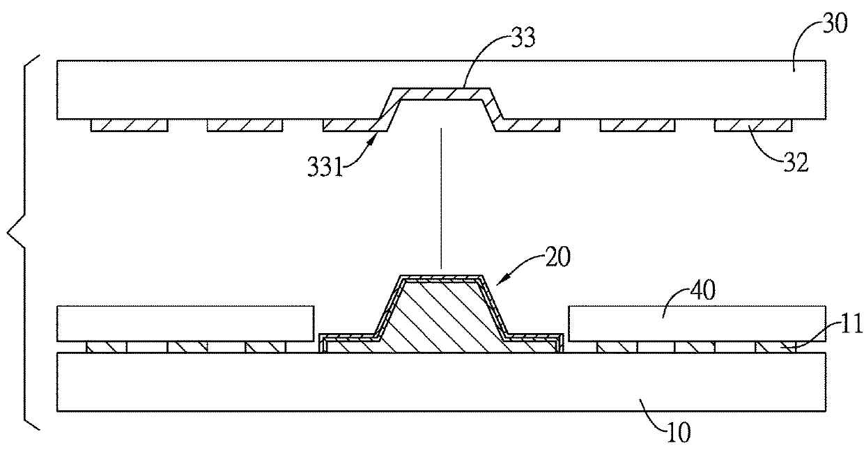
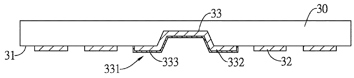
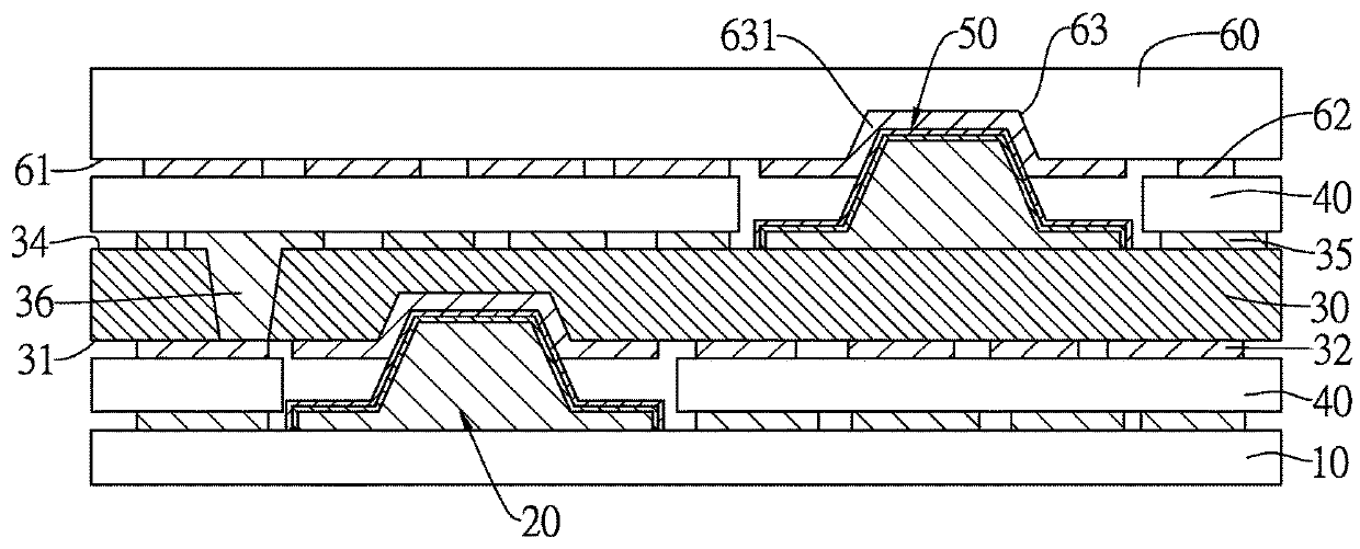
[0022]With reference to FIG. 1A, a multi-layer circuit board in accordance with the present invention includes multiple circuit boards that are stacked to each other and includes a first circuit board 10, multiple first conducting blocks 20, a second circuit board 30 and an insulating layer 40.

[0023]With reference to FIG. 1B, the first circuit board 10 has a first conductor layer 11 formed on a surface of the first circuit board 10. A width of a cross-sectional area of each first conducting block 20 progressively decreases in an upward direction from the surface of the first circuit board 10, such that a top area of the first conducting block 20 is less than a bottom area of the first conducting block 20. Each first conducting block 20 has a base layer 21, a strengthening layer 22 and an anti-oxidant layer 23.

[0024]The base layer 21 is mounted on the surface of the first circuit board 10 and adjoins the first conductor layer 11. Each first conducting block 20 is electrically connect...


PUM


Abstract

A multi-layer circuit board includes a first circuit board, multiple conducting blocks, a second circuit board, and multiple conducting recesses. The first circuit board has a first conductor layer formed thereon. The conducting blocks are mounted on the first circuit board and electrically connected to the first conductor layer. The second circuit board has a second conductor layer mounted thereon and facing the first circuit board. The conducting recesses are formed in the surface of the second circuit board. Each conducting recess has a conducting layer electrically connected to the second conductor layer. When the conducting blocks are mounted in the conducting recesses, the first conductor layer and the second conductor layer are electrically connected through the conducting blocks and the conducting recesses. As can be separated from the first circuit board for test of the two conductor layers, the yield of the second circuit board is enhanced.

Description

BACKGROUND OF THE INVENTION1. Field of the Invention[0001]The present invention relates to a circuit board and, more particularly, to a multi-layer circuit board facilitating test thereof with conductor layers electrically connected to each other through conducting blocks and conducting recesses formed between each adjacent two boards of the multi-layer circuit board.2. Description of the Related Art[0002]Circuit boards are products built to reduce the need of wires connected between electronic components and to lower the production cost. As circuits become more and more complicated, the use of multi-layer circuit boards has become commonplace in the electronics industry. With reference to FIGS. 3A and 3B, a conventional multi-layer circuit board includes a first substrate 70, a first conductor layer 71, a second substrate 80 and a second conductor layer 81. The first conductor layer 71 is formed on the first substrate 70. The first conductor layer 71 may be formed by performing pho...

Claims


Application Information

Patent Timeline
Patent Type & Authority Patents(United States)
IPC IPC(8): H05K1/09H05K1/02
CPCH05K1/0298H05K1/09H05K1/144H05K3/4614H05K2201/0367H05K2201/042H05K2201/09472
Inventor LIN, TING-HAOCHANG, CHIAO-CHENGLIN, YI-NONG
Owner KINSUS INTERCONNECT TECH
Why Eureka
Try Eureka