Reactor and method of processing a semiconductor substrate

a technology of semiconductor substrate and reaction chamber, which is applied in the direction of heat measurement, optical radiation measurement, instruments, etc., can solve the problems of reducing the strength of the substrate, affecting the accuracy and the use of contact probes such as thermocouples or resistance wire thermometers, etc., to achieve accurate determination of the temperature of the substrate during processing

Inactive Publication Date: 2002-02-12
KOKUSAI SEMICON EQUIP CORP
View PDF13 Cites 195 Cited by
  • Summary
  • Abstract
  • Description
  • Claims
  • Application Information

AI Technical Summary

Benefits of technology

This patent describes an improved reactor design that has several benefits compared to previous designs. It includes a special sensor that measures how hot the surface of a material is when it's being processed. This helps ensure accurate results even after the process is complete. Additionally, this new rector also allows for better control over what gases are added to the materials while they're being heated up. By doing this, researchers don't have to worry about other substances getting onto their equipment and affecting the data they collect. Overall, these improvements make the reactor much easier to use and get better results out of every experiment.

Problems solved by technology

The technical problem addressed in this patent text needs to be identified by a senior R&D person who has read it through.

Method used


Image

  • Reactor and method of processing a semiconductor substrate
  • Reactor and method of processing a semiconductor substrate
  • Reactor and method of processing a semiconductor substrate

Examples


Embodiment Construction

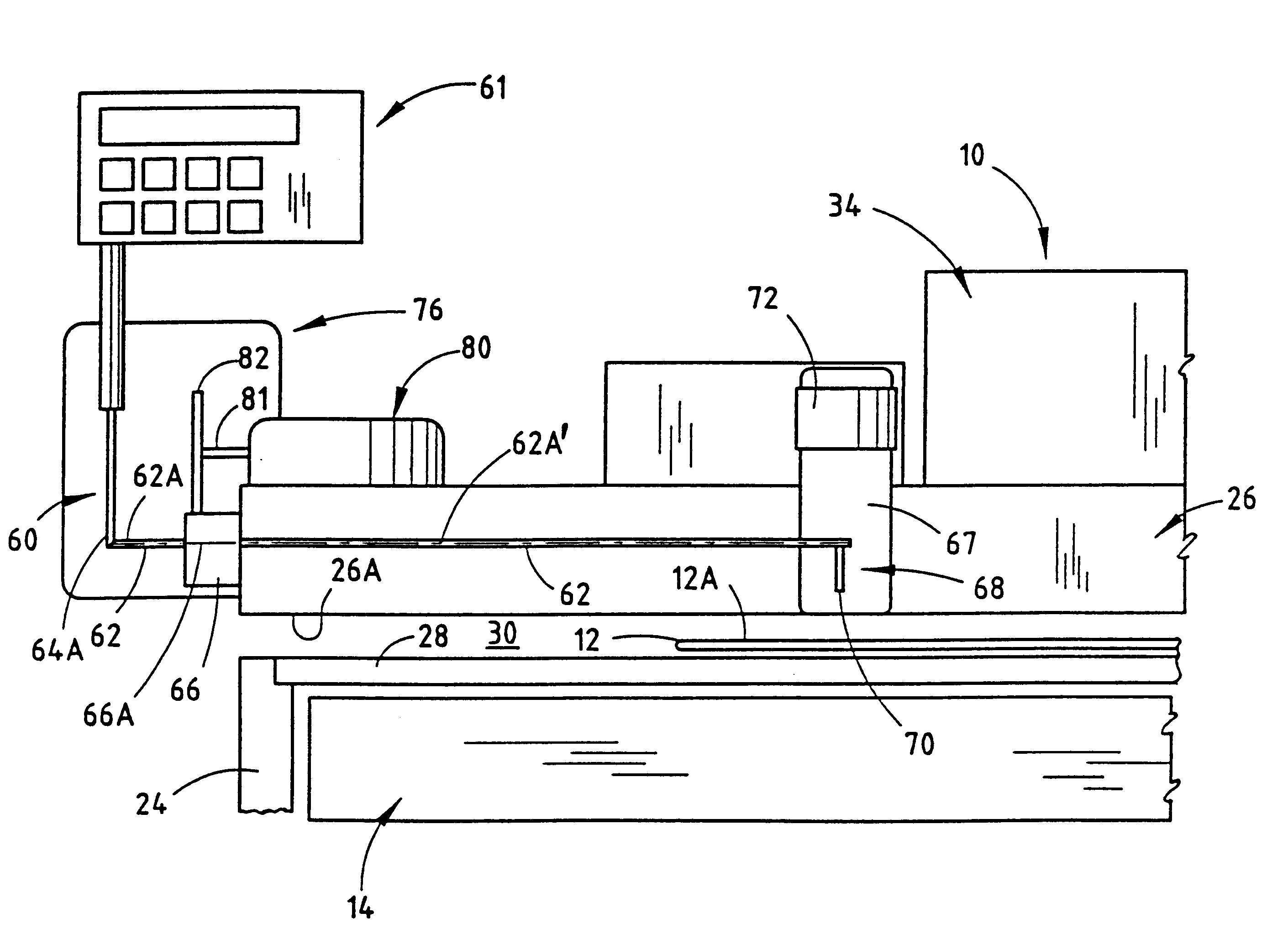
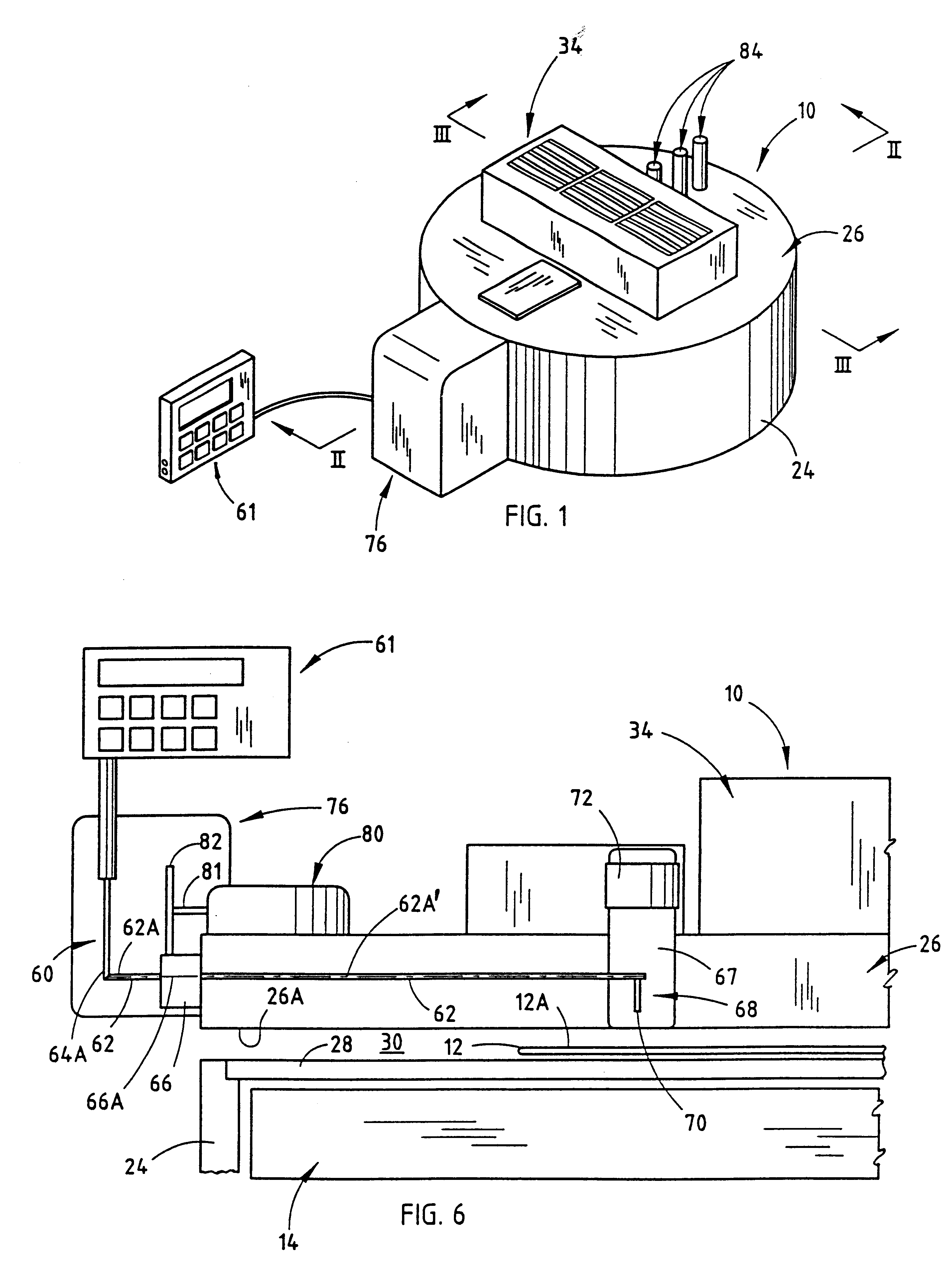
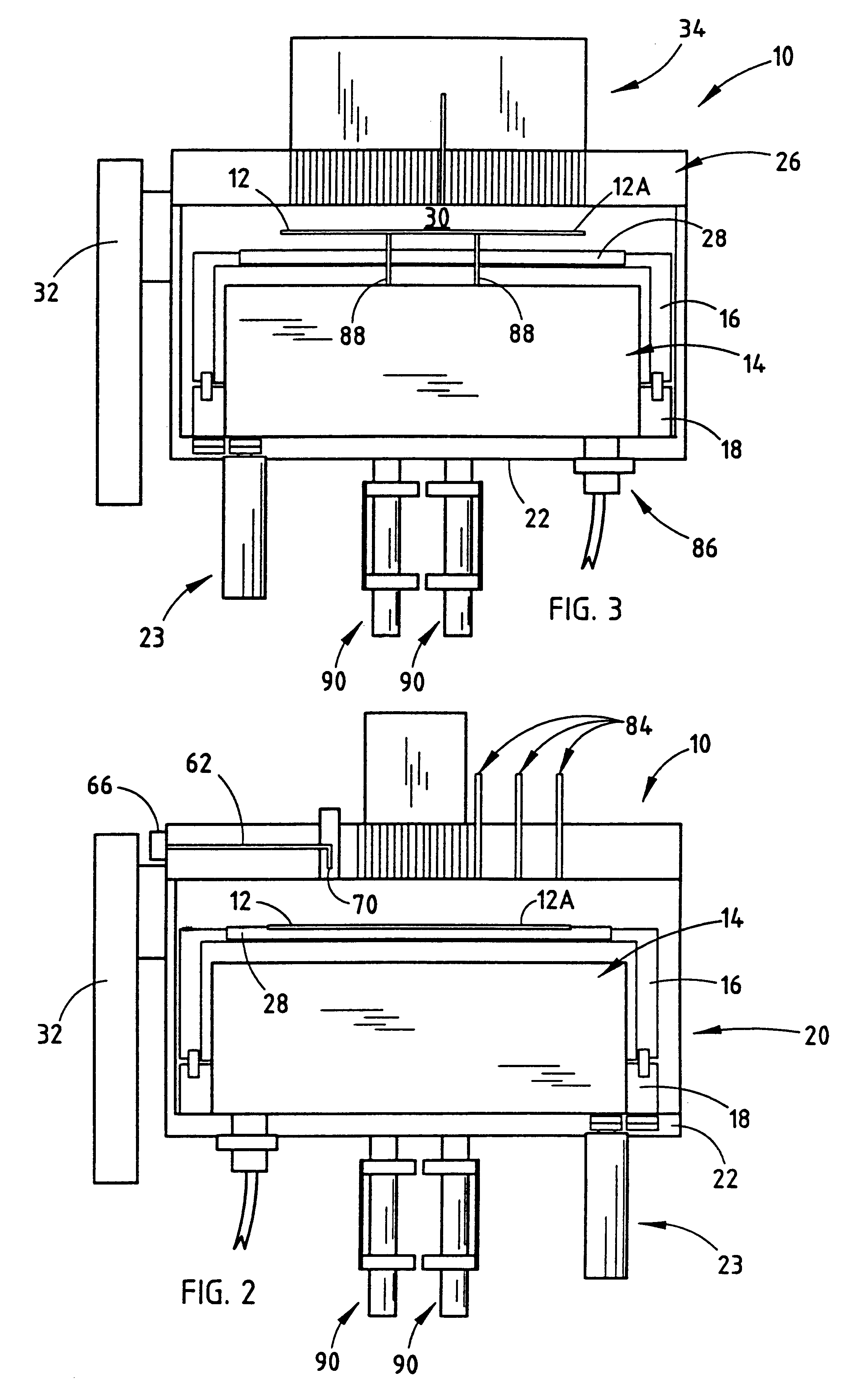
Referring now to the drawings and particular to FIGS. 1 and 2, a reactor for processing semiconductor substrates is generally indicated by the numeral 10. In the illustrated embodiment, reactor 10 comprises a single wafer processing reactor that is suitable for performing various fabrication processes on a semiconductor substrate 12, such as a semi-conductor wafer. Reactor 10 is particularly suitable for thermal processing of a semiconductor wafer. Such thermal processes include thermal annealing of a semiconductor wafer and thermal reflow of boro-phosphorous gasses, and chemical vapor deposition of thin film applications, such as high temperature oxide, low temperature oxide, high temperature nitride, doped and undoped polysilicon, silicon epitaxial and tungsten metal and tungsten silicide films, in the fabrication of a semiconductor device. The control of these processes depends on the control of gas flow, gas pressure, and wafer temperature. As will be described in more detail, r...


PUM

PropertyMeasurementUnit
Angleaaaaaaaaaa
Temperatureaaaaaaaaaa
Flow rateaaaaaaaaaa

Abstract

A reactor for processing a substrate includes a first housing defining a processing chamber and supporting a light source and a second housing rotatably supported in the first housing and adapted to rotatably support the substrate in the processing chamber. A heater for heating the substrate is supported by the first housing and is enclosed in the second housing. The reactor further includes at least one gas injector for injecting at least one gas into the processing chamber onto a discrete area of the substrate and a photon density sensor extending into the first housing for measuring the temperature of the substrate. The photon density sensor is adapted to move between a first position wherein the photon density sensor is directed to the light source and a second position wherein the photon density sensor is positioned for directing toward the substrate. Preferably, the communication cables comprise optical communication cables, for example sapphire or quartz communication cables. A method of processing a semiconductor substrate includes supporting the substrate in a sealed processing chamber. The substrate is rotated and heated in the processing chamber in which at least one reactant gas is injected. A photon density sensor for measuring the temperature of the substrate is positioned in the processing chamber and is first directed to a light, which is provided in the chamber for measuring the incident photon density from the light and then repositioned to direct the photon density sensor to the substrate to measure the reflection of the light off the substrate. The incident photon density is compared to the reflected light to calculate the substrate temperature.

Description


Claims


Application Information

Patent Timeline
Owner KOKUSAI SEMICON EQUIP CORP
Why Eureka
Try Eureka