Crystal circle center correcting device and correcting method

A calibrator and wafer technology, applied in semiconductor/solid-state device manufacturing, semiconductor/solid-state device testing/measurement, electrical components, etc., can solve problems such as uneven wafer response, and achieve rapid and improved wafer center calibration methods Uniformity, the effect of solving the non-uniformity of wafer reaction

Inactive Publication Date: 2007-10-03
WINBOND ELECTRONICS CORP
View PDF5 Cites 0 Cited by
  • Summary
  • Abstract
  • Description
  • Claims
  • Application Information

AI Technical Summary

Problems solved by technology

[0007] In summary, the wafer center corrector of the present invention includes at least one arc-shaped bottom rib of the wafer center corrector, the radius of curvature of the arc-shaped bottom rib is the same as that of the electrostatic chuck and the focus ring, and the bottom rib The thickness and width correspond to the approximate annular gap formed by the electrostatic chuck and the focus ring. When in use, the wafer center corrector is placed on the electrostatic chuck and the focus ring, so that the bottom of the wafer center corrector is placed into the electrostatic chuck and focused. In the approximate annular gap formed by the ring, then rotate the wafer center corrector to make the bottom rib rotate once in the approximate annular gap formed by the electrostatic chuck and the focus ring. During the rotation process, the bottom rib of the wafer center corrector and the electrostatic chuck and The friction, contact and movement between the focus rings can maintain a good and uniform annular gap between the electrostatic chuck and the focus ring, which greatly improves the uniformity of the wafer reaction in the reaction chamber; in addition, the wafer center correction method of the present invention is fast and simple , in an economical and effective way to solve the problem of uneven wafer response caused by artificial assembly differences of electrostatic chucks and focus rings

Method used


Image

  • Crystal circle center correcting device and correcting method
  • Crystal circle center correcting device and correcting method
  • Crystal circle center correcting device and correcting method

Examples


Embodiment Construction

[0018] The preferred embodiment of the wafer center corrector proposed by the present invention will be described in detail as follows. However, in addition to the detailed description, the present invention can also be widely implemented in other embodiments, and the scope of the present invention is not limited. The patent scope of the claims of the present invention shall prevail.

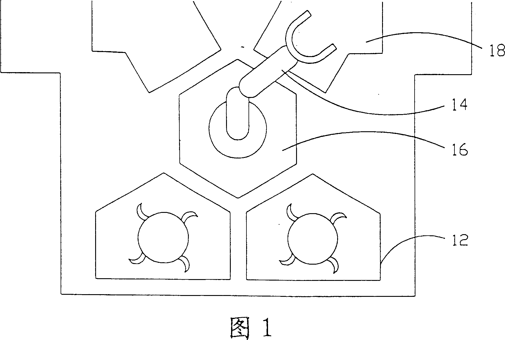
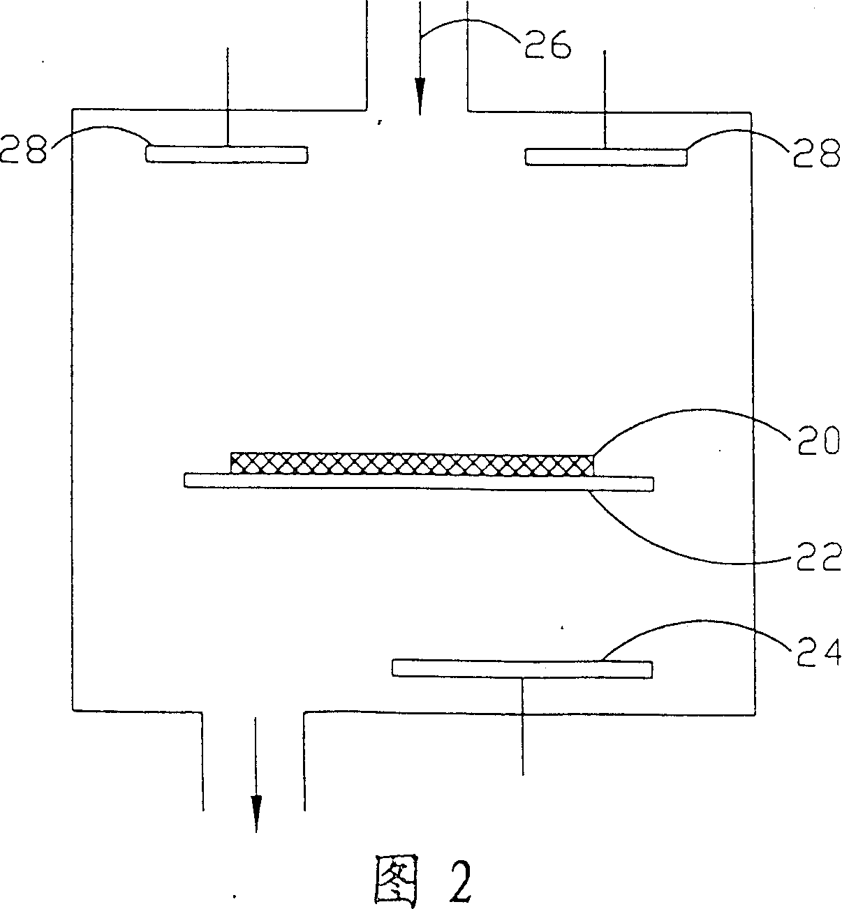
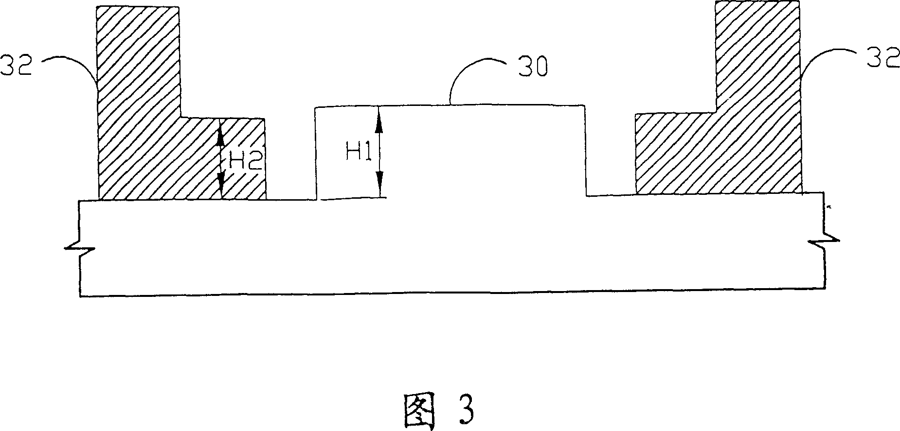
[0019] The wafer center corrector of the present invention is used to correct the assembly error of the focus ring in the etching or deposition reaction chamber, and it at least includes an arc-shaped bottom rib of the wafer center corrector, and the radius of curvature of the arc-shaped bottom rib is consistent with that of the electrostatic chuck and The radius of curvature of the focus ring is the same. When in use, the wafer center corrector is placed on the electrostatic chuck and the focus ring, so that the bottom rib of the wafer center corrector is placed in the approximate annular gap fo...


PUM


Abstract

The corrector is utilized to correct error of assembling static suction cup and focus ring. The focus ring in ring structure with L shaped cross section hitches the static suction cup. First and second ring walls are located at L shaped upper and lower parts respectively. The corrector comprises a body and a curved bottom rib. The radius of curvature of the bottom rib is same as the radius of curvature of the static suction cup and the focus ring. Width of bottom rib is equal to gap between first ring wall and static suction cup, and the bottom rib can be put into the ring gap. Thickness of the bottom rib is larger than the thickness of the first ring wall. The invention keeps a even ring gap between the static suction cup and focus ring, raises uniformity of reaction in reaction chamber to solve the issue of inhomogeneity of wafer reaction caused by error of assembling static suction cup and focus ring.

Description

technical field [0001] The invention relates to semiconductor manufacturing technology, in particular to a wafer center corrector and a calibration method for wafer deposition or wafer etching machines. Background technique [0002] With the advent of the 21st century, the technology of the semiconductor industry has also continued to develop. Not only has it already entered the sub-micron era, but it will also move towards the nanometer era in the future. In response to the trend of electronic products becoming smaller and more functional, not only the wafer size in the semiconductor manufacturing process has moved from 8 inches to the current 10-inch wafer, but the process line width has also changed from the original 0.18 micron process. Reaching today's 0.13 micron process. Along with the trend of larger and larger chips and smaller and smaller components, there are technical requirements for various links in the manufacturing process. It is conceivable that because th...

Claims


Application Information

Patent Timeline
Patent Type & Authority Patents(China)
IPC IPC(8): H01L21/66H01L21/00
Inventor 陈复生
Owner WINBOND ELECTRONICS CORP
Why Eureka
Try Eureka