Improved method for etching vias

An etching and substrate technology, which is applied in the field of plasma processing, can solve the problems such as the serious impact of 150mm substrate, and achieve the effects of reducing residence time, reducing the formation of columns, and eliminating the formation of columns

Inactive Publication Date: 2007-10-24
UNAXIS USA
View PDF2 Cites 0 Cited by
  • Summary
  • Abstract
  • Description
  • Claims
  • Application Information

AI Technical Summary

Problems solved by technology

This problem will be more severe for 150mm substrates compared to the 3 inch substrates used by Nam et al.

Method used


Image

  • Improved method for etching vias
  • Improved method for etching vias
  • Improved method for etching vias

Examples


Embodiment Construction

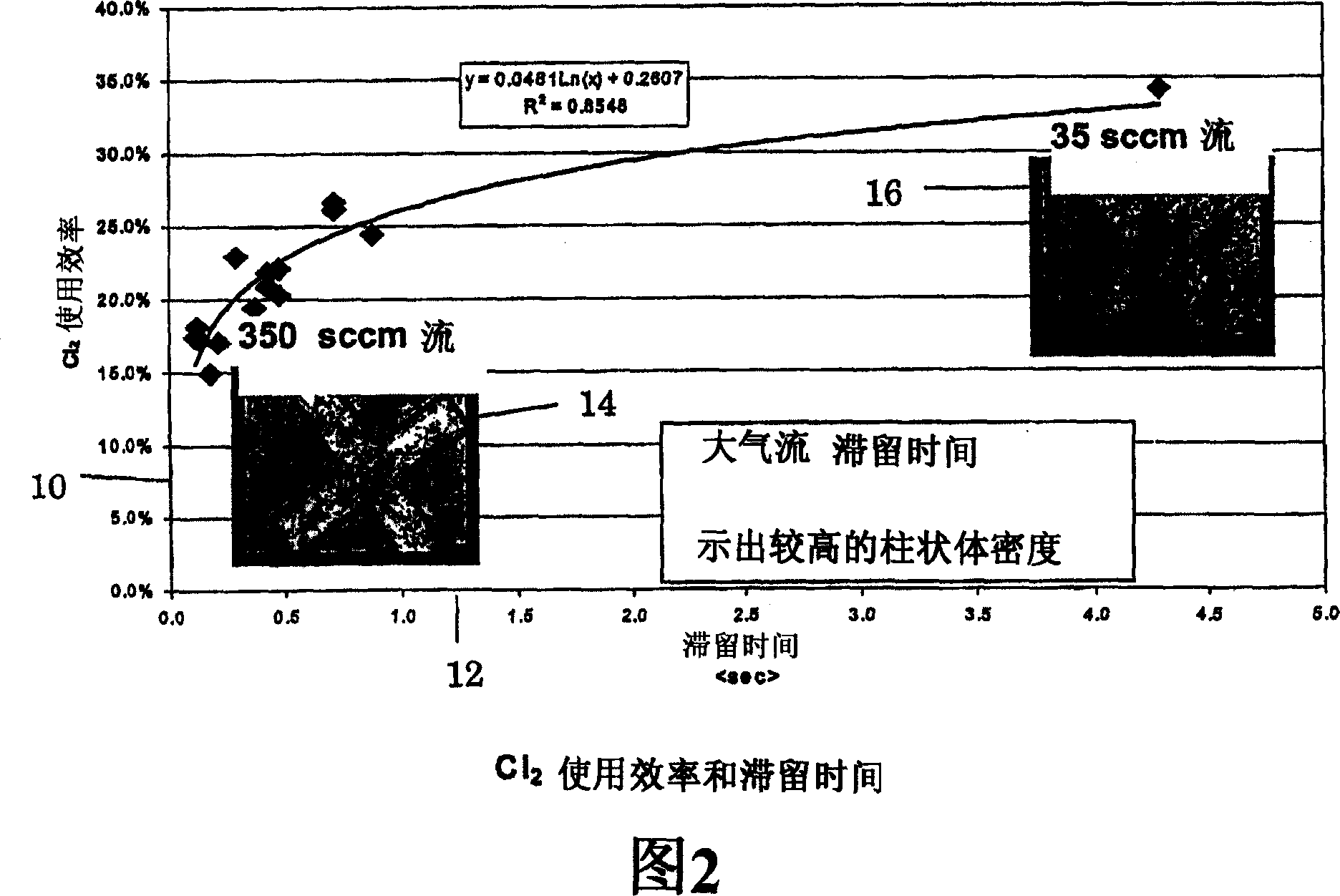
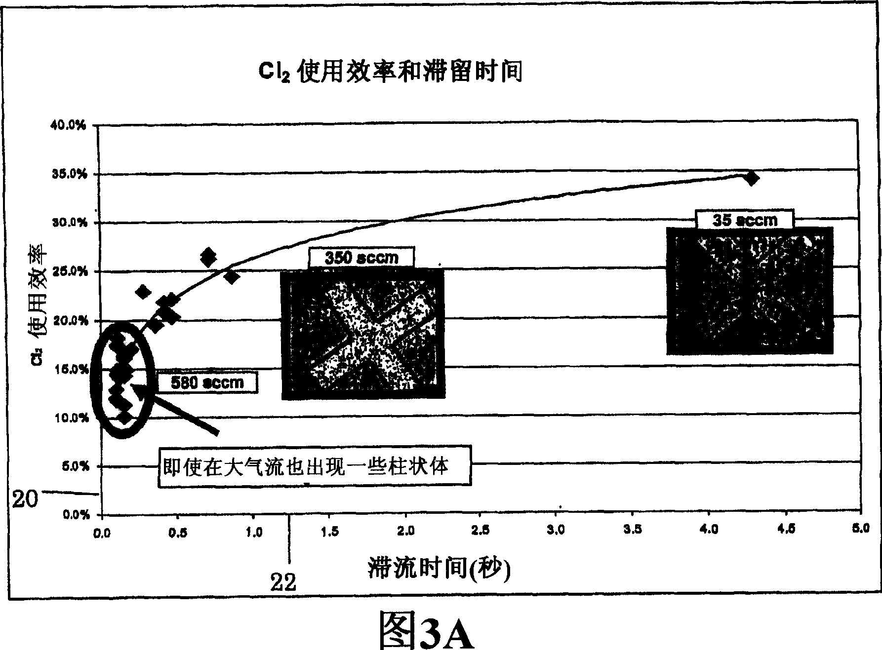
[0034] Preferred embodiments of the present invention are directed to a method utilizing high-speed Cl 2 Gas flow (short dwell time), high inductively coupled plasma (ICP) power, ICP confinement ring, low RF bias etch initiation and RF jump to etch GaAs vias. Discussed in more detail below, these process modifications result in a high-speed (>6 μm / min) via etch process that eliminates pillars. In addition, a sloped via profile is obtained by etching a sloped photoresist mask.

[0035] Dry etching of GaAs vias requires etching relatively deep (~100 μm) features into the thinned GaAs substrate, terminating on a metal etch stop layer (typically gold). As shown in Table 1, due to the relatively high volatility of the etch products, dry etch processes are typically chlorine-based (i.e., BCl 3 / Cl 2 , Ar / Cl 2 , SiCl 4 / Cl 2 Wait). Although fluorine plasma does not chemically corrode GaAs, it can also contain a small amount of precursor (CF 4 etc.) Fluorine is added to the tr...


PUM


Abstract

An improved method for etching a substrate that reduces the formation of pillars is provided by the present invention. In accordance with the method, the residence time of an etch gas utilized in the process is decreased and the power of an inductively coupled plasma source used to dissociate the etch gas is increased. A low bias RF voltage is provided during the etching process. The RF bias voltage is ramped between different bias levels utilized during the etch process. An inductively coupled plasma confinement ring is utilized to force the reactive species generated in the inductively coupled plasma source over the surface of the substrate. These steps reduce or eliminate the formation of pillars during the etching process.

Description

[0001] This application claims priority to and commonly owns U.S. Provisional Patent Application No. 60 / 371,056, filed April 9, 2002, and entitled "Improved Method for Etching Via Holes," which provisional patent is incorporated herein by reference Apply. technical field [0002] The present invention generally relates to plasma processing of a substrate. More specifically, the present invention relates to an improved method for etching vias in the backside of a gallium arsenide substrate in a plasma processing chamber. Background technique [0003] In the wireless communication industry, GaAs devices are widely used, and the high electron mobility of GaAs makes it very suitable for high frequency, low noise, high gain applications. Although it has very good electrical characteristics, GaAs has relatively poor thermal conductivity, making it difficult to eliminate the thermal influence of power devices. The usual solution to this problem is to form vias from the backside o...

Claims


Application Information

Patent Timeline
Patent Type & Authority Patents(China)
IPC IPC(8): H01L21/302H01L21/3065H01L21/00H01L21/306H01L21/308
CPCH01L21/3065Y10S438/935H01L21/67069H01J37/32082H01L21/308H01L21/30621H01J37/32706
Inventor 罗素·韦斯特曼大卫·J·约翰逊
Owner UNAXIS USA
Why Eureka
Try Eureka