Unlock instant, AI-driven research and patent intelligence for your innovation.

Flash memory storage unit and its mfg. method

A technology for flash memory storage and manufacturing methods, which is applied to the structure of flash memory storage units and its manufacturing field, and can solve problems such as multi-time and cost

Inactive Publication Date: 2008-01-09
POWERCHIP SEMICON CORP
View PDF2 Cites 0 Cited by
  • Summary
  • Abstract
  • Description
  • Claims
  • Application Information

AI Technical Summary

Problems solved by technology

[0004] Although the known split gate design can effectively avoid the problems caused by over-erasing, since the select gate is formed after the floating gate is formed, the manufacturing process of the split gate requires two polysilicon deposition steps, thus requiring more time consuming

Method used


Image

  • Flash memory storage unit and its mfg. method
  • Flash memory storage unit and its mfg. method

Examples


Embodiment Construction

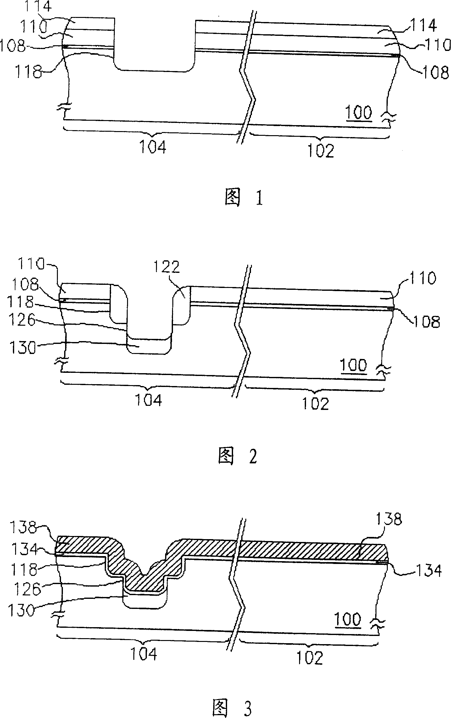
[0027] The flash memory manufacturing process of the preferred embodiment of the present invention will be described below with reference to FIGS. 1-6 , but the description of the preferred embodiment and FIGS. 1-6 are not intended to limit the scope of the present invention.

[0028] Referring to FIG. 1 , firstly, a substrate 100 is provided, which is divided into a peripheral circuit area 102 and a memory cell area 104 . Next, a thermal oxide layer 108 and a hard mask layer 110 are sequentially formed on the substrate 100, wherein the formation method of the thermal oxide layer is, for example, thermal oxidation (Thermal Oxidation), and the material of the hard mask layer 110 is, for example, nitride Silicon, which is formed by, for example, SiH 2 Cl 2 / NH 3 Low-pressure chemical vapor deposition (LPCVD) of reactive gases. Next, a patterned photoresist layer 114 is formed on the hard mask layer 110, and then the exposed hard mask layer 110 is etched away using the photore...


PUM


Abstract

The present invention provides a flash memory storage unit and its making method. Said flash memory storage unit includes substrate, selection gate, floating gate, gate dielectric layer, high-voltage doped region and source region. On the substrate it has first opening, also has second opening. The selection gate is positioned on side wall of first opening, the floating gate is positioned on side wall of second opening, and the gate dielectric layer is positioned between selection / floating gate and substrate. The high voltage doped region is positioned in substrate of bottom portion of second opening, and the source region is positioned in the substrate of outer side of first opening. In the making method the selection gate and floating gate are respectively and simultaneously formed on the side walls of first opening and second opening.

Description

technical field [0001] The invention relates to a structure of a semiconductor element and a manufacturing method thereof, in particular to a structure of a flash memory cell (Flash Memory Cell) and a manufacturing method thereof. Background technique [0002] A typical flash storage unit is composed of a stack structure of a control gate and a floating gate, and source / drain electrodes on both sides thereof, wherein the material of the control gate and the floating gate is generally polysilicon. In a common method of operating a flash memory cell, a high positive voltage is applied to the control gate during writing so that electrons are injected into the floating gate so that the channel below the floating gate does not conduct When erasing, a high negative voltage is applied to the control gate to expel electrons from the floating gate, so that the channel under the floating gate can be turned on during reading, and the data value of the memory cell It is judged by wheth...

Claims


Application Information

Patent Timeline
Patent Type & Authority Patents(China)
IPC IPC(8): H01L27/10H01L27/115H01L21/8239H01L21/8247H10B69/00H10B99/00
Inventor 张格荥许汉杰
Owner POWERCHIP SEMICON CORP