

Method and apparatus for endpoint detection using partial least squares
A technology of endpoints and equipment, applied in the field of endpoint detection, which can solve problems such as strict requirements and lack of mathematics
- Summary
- Abstract
- Description
- Claims
- Application Information
AI Technical Summary
Problems solved by technology
Method used
Image

Examples
Embodiment Construction
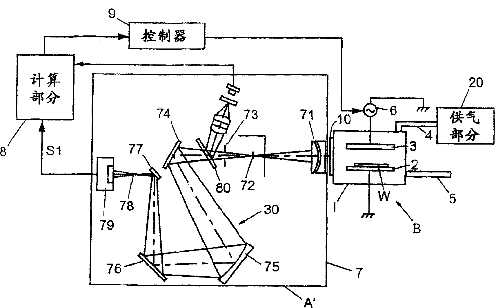
[0034] As noted above, the present inventors have recognized problems with conventional fabrication of reaction chambers and methods of using those reaction chambers that can be addressed by use of the present invention. Accordingly, the present invention provides an improved apparatus and method for endpoint detection that overcomes the disadvantages associated with conventional processing chambers.
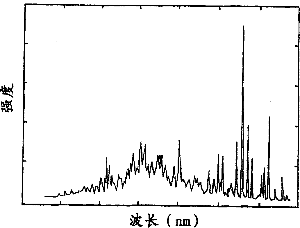
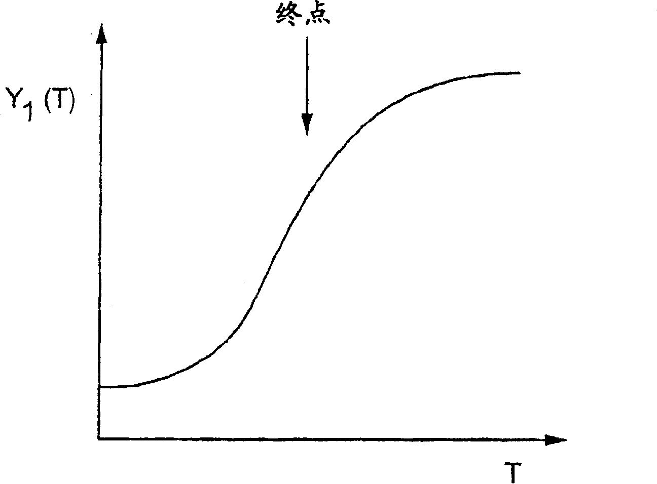
[0035] The inventors have recognized that it is difficult to accurately detect the endpoint of an etch process for a substrate with a small opening area. As the device size decreases, the opening area decreases, and the endpoint signal and signal-to-noise ratio decrease accordingly. What is needed is a simplified multivariate analysis method for selecting endpoint signals using known physical criteria set by the etch process.
[0036] In addition, the inventors have realized that it is difficult to repeatedly detect the endpoint for the etch process of different wafers. The en...
PUM
 Abstract
Description
Claims
Application Information