Structure for encapsulating semiconductor

A packaging structure and semiconductor technology, which is applied in semiconductor devices, semiconductor/solid-state device parts, electric solid-state devices, etc., can solve problems affecting accuracy, negative impact on packaging pass rate, structural deformation and distortion, etc.

Active Publication Date: 2008-04-16
HARVATEK CORPORATION
View PDF4 Cites 0 Cited by
  • Summary
  • Abstract
  • Description
  • Claims
  • Application Information

AI Technical Summary

Problems solved by technology

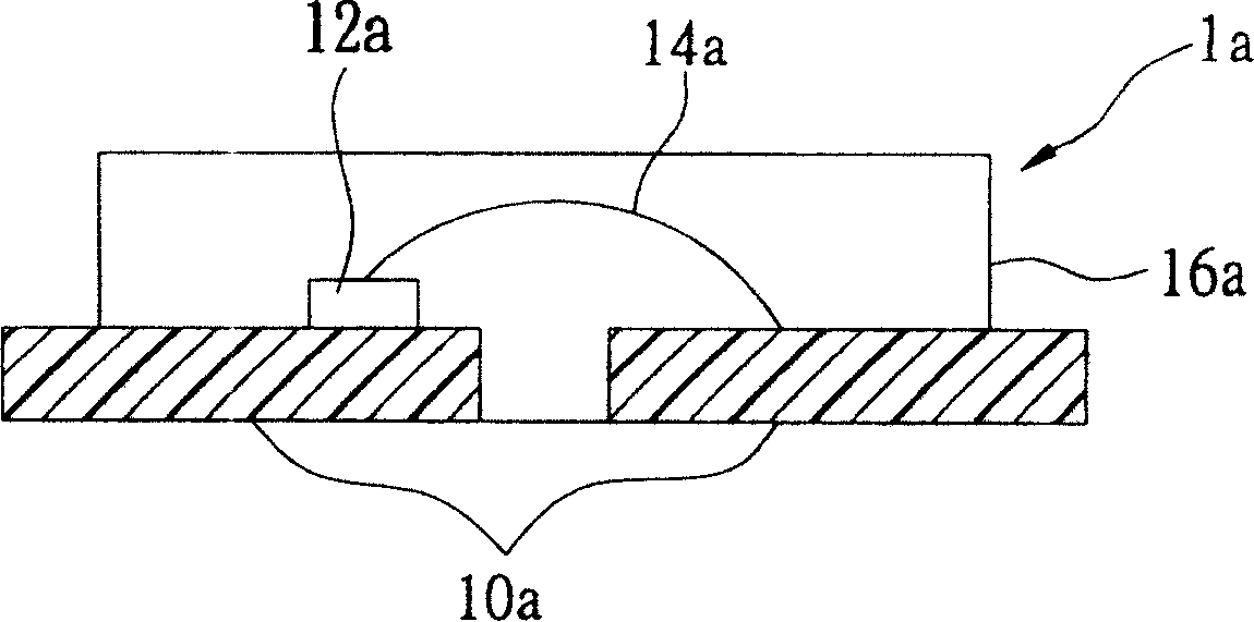
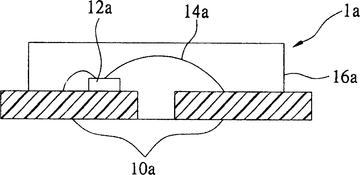
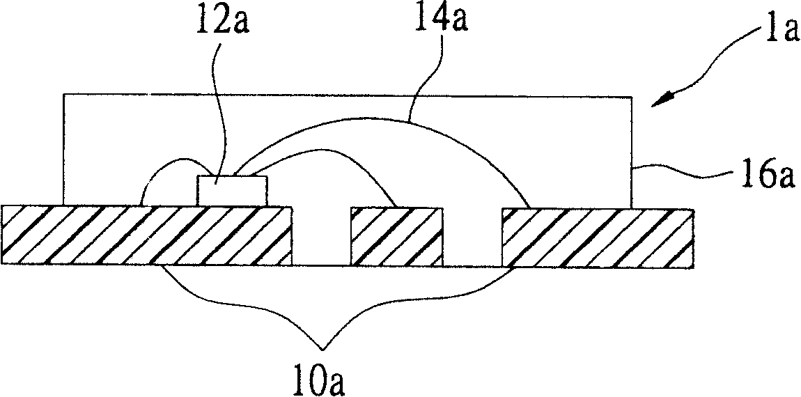
[0004] Please refer to Figure 1A to Figure 1C , for the existing LED packaging structure 1a, the substrate 10a is bonded to the LED chip 12a, and connected to the wire 14a and packaged with the packaging material 16a (may have multiple grooves), especially when facing assembly, the traditional The light-emitting diode packaging structure 1a faces relatively difficult problems of structural strength and brightness, such as structural deformation and distortion when cutting the substrate (which often occurs when the substrate is too thin), which will affect the accuracy in practical applications and also have a negative impact on the packaging yield. influences

Method used


Image

  • Structure for encapsulating semiconductor
  • Structure for encapsulating semiconductor
  • Structure for encapsulating semiconductor

Examples


Embodiment Construction

[0043] Please refer to Figure 2A to Figure 2B , Where the gap is W (the middle of the substrate 10) and the thickness is H, that is, H is proportional to W, when Figure 2A The thinner the thickness of the plate, the smaller the interval, that is Figure 2A The thickness of each layer is 1 / 2, such as Figure 2B The stacked structure, Figure 2B The thin layer spacing can be very small to achieve the purpose of narrowing the spacing and strengthening the board. Therefore, according to the aforementioned relationship of H to W, the structure of the stack layer is not necessarily 1 / 2, which can be adjusted according to actual needs.

[0044] Please refer to Figure 3A to Figure 3B , Figure 4 , Figure 5A Figure 5E is an embodiment of the present invention, where Figure 3A and Figure 3B It is a single-sided stacked type, Figure 4 For double-sided stacking, Figure 5A To FIG. 5E is an embodiment with an outer frame device 17 (the outer frame device 17 in FIG. 5D and FIG. 5E may be ...


PUM


Abstract

Related to encapsulating structure for semiconductor, the invention includes following parts: basis material of having positive and negative faces; semiconductor setup on the positive and negative faces of the basis material; outline border set made from opaque material on the basis material, and around the semiconductor; high molecular obsturator in use for filling up the outline border set, and capable of letting light source pass in or out of the obsturator. Advantages are: easy of setting procedures, low cost for adding devices, good mechanical strength of basis material; usable traditional encapsulation equipment, and high luminous brightness.

Description

Technical field [0001] The invention relates to a package structure of a semiconductor or a light-emitting body, and in particular to a package structure with high intensity and light transmission without interference from external light, and is not easy to deform, increases the pass rate and quality of the package, and uses light-emitting diodes When the chip is packaged, it is easy to meet the packaging requirements required by the electronic chip, and it is better than the existing substrate structure and has a low installation cost. The method of double-layer substrate is mainly used to improve the strength characteristics of the substrate and the outer frame device prevents the outside Light interference; and a packaging structure of optoelectronic semiconductors that is more excellent than the existing luminous body packaging structure. Background technique [0002] In the packaging industry, semiconductor packaging is the focus of attention. The light-emitting diode (LED) ...

Claims


Application Information

Patent Timeline
Patent Type & Authority Patents(China)
IPC IPC(8): H01L23/31H01L33/00H01L31/18H01L33/48
CPCH01L2224/48091H01L2224/48247H01L2224/48257Y02P70/50H01L2924/00014
Inventor 汪秉龙庄峰辉洪基纹林川发
Owner HARVATEK CORPORATION
Why Eureka
Try Eureka