


Quick Research
Generate reliable direction feasibility study reports for your R&D in just a few steps.

Technical Q&A
Discover and master advanced knowledge NOW. Basics, ideas, possibilities, all at once.

Find Solutions
As an expert in R&D theories, this can generate solutions to your technical problems instantly.

Evaluate Feasibility
Analyze your overall solution with one click, know your potential R&D risks in advance.

Monitor Landscape
Get weekly tech updates, stay abreast of the latest tech innovations and key insights.
Method for improving CMP process window of deep slot DRAM tungsten metal bit line
A deep trench and bit line technology, applied in electrical components, semiconductor/solid-state device manufacturing, circuits, etc., can solve the problems of uneven grinding of tungsten metal, affecting the performance of tungsten metal process window, etc., and achieve the effect of preventing the impact.
- Summary
- Abstract
- Description
- Claims
- Application Information
AI Technical Summary
Problems solved by technology
Method used
Image

Examples
Embodiment Construction
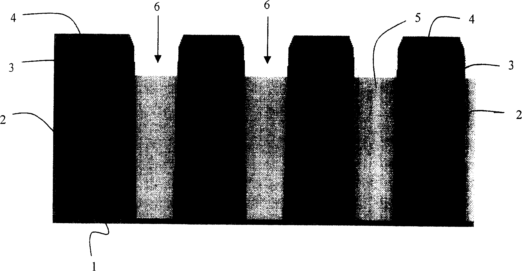
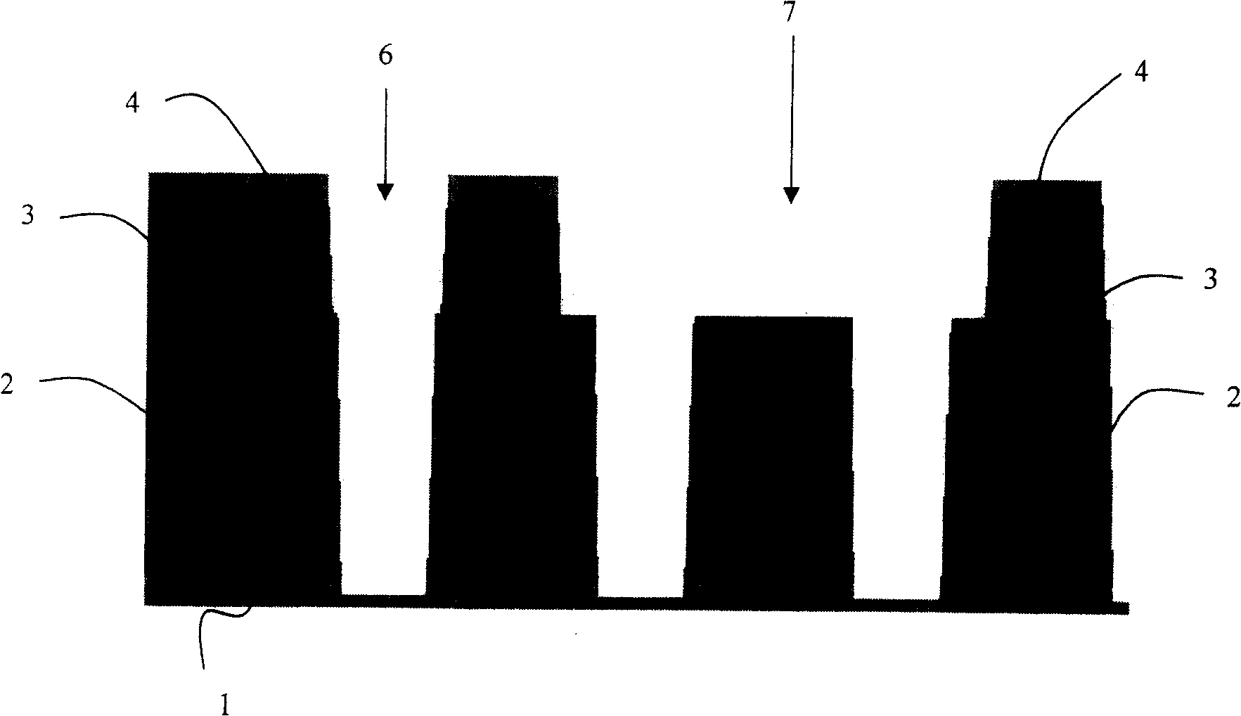
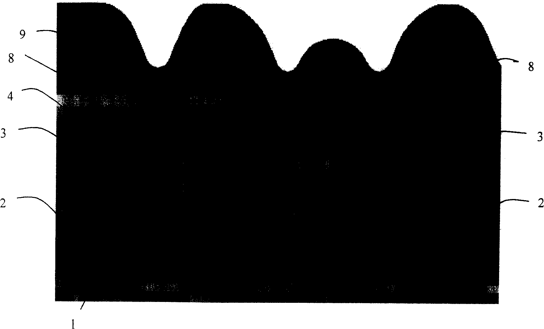
[0024] In the manufacturing process of deep trench DRAM, the conventional process of forming contact window tungsten plugs, such as Figure 1A-1D As shown, after the character line 1 is formed, it is covered with the first dielectric layer 2, the second dielectric layer 3, and the polysilicon layer 4; the photoresist defines the bit line contact window pattern, and the polysilicon layer 4 is used as an etching barrier layer for etching. The etching of the bit line contact window forms the bit line contact window 6, then fills the contact window with photoresist, carries out recess etching, forms the plug 5 of photoresist to protect the bottom of the contact window from being in the subsequent bit line formation process Affected. The photoresist recess (ARCRecess) etching of the conventional (M0) bit line contact window 6 only considers the shape of the pattern, so the polysilicon layer 4 as the etching barrier remains, as Figure 1A shown. Then form an anti-reflection layer a...
PUM
 Abstract
Description
Claims
Application Information
 - R&D Engineer
- R&D Manager
- IP Professional
- Industry Leading Data Capabilities
- Powerful AI technology
- Patent DNA Extraction
Browse by: Latest US Patents, China's latest patents, Technical Efficacy Thesaurus, Application Domain, Technology Topic, Popular Technical Reports.
© 2024 PatSnap. All rights reserved.Legal|Privacy policy|Modern Slavery Act Transparency Statement|Sitemap|About US| Contact US: help@patsnap.com