Slave device, master device and stacked device
A technology of slave devices and stacked devices, which is applied in the fields of climate sustainability, semiconductor devices, information technology support systems, etc., and can solve the problems of complex manufacturing process and difficult to form with high precision.
- Summary
- Abstract
- Description
- Claims
- Application Information
AI Technical Summary
Problems solved by technology
Method used
Image

Examples
no. 1 Embodiment approach example
[0097] (Outline of lamination device)
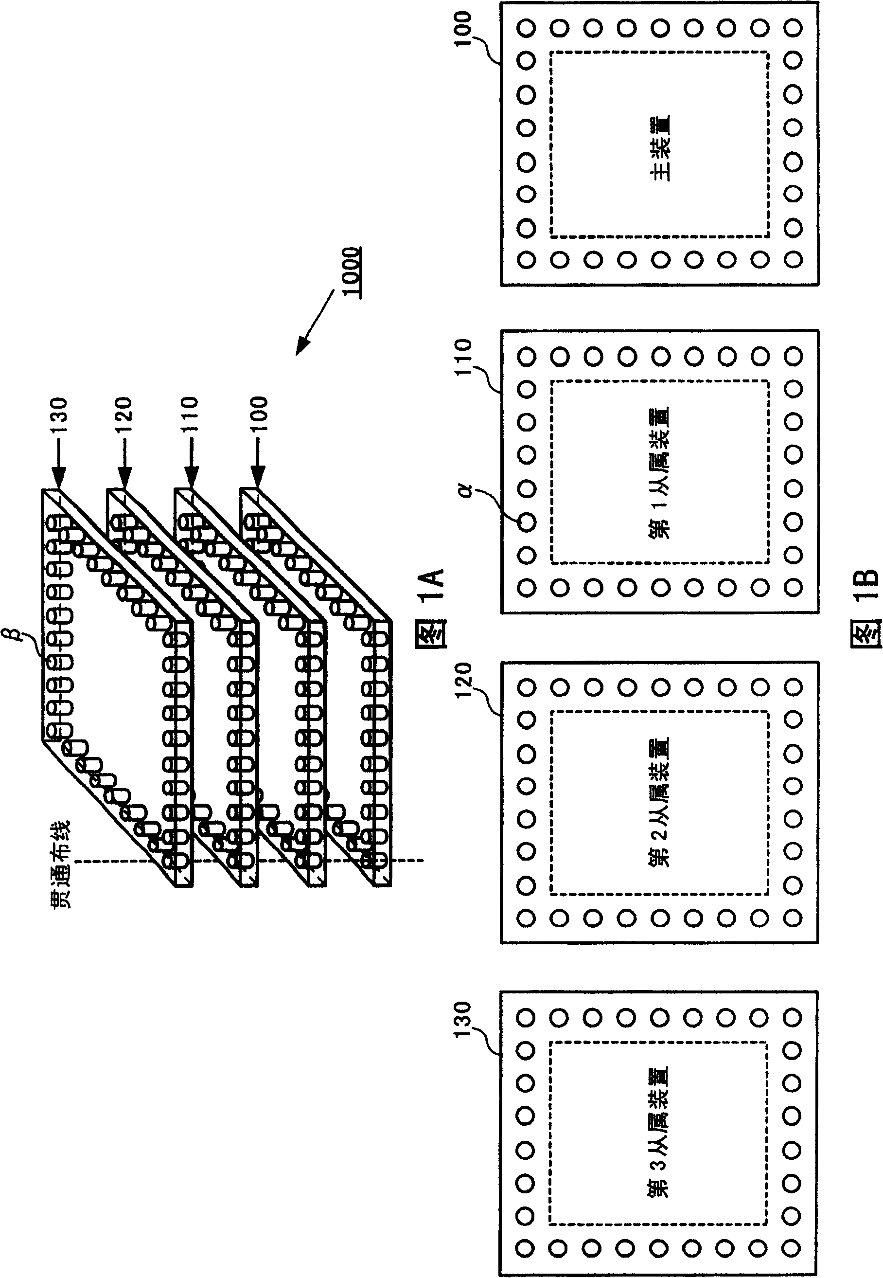
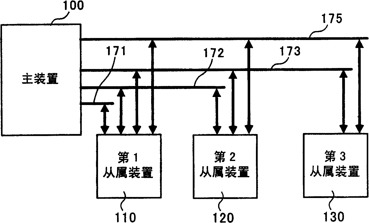
[0098]FIG. 1A is a schematic diagram of a lamination device according to a first embodiment of the present invention, and FIG. 1B is a schematic diagram showing terminal configurations of a slave device and a master device in FIG. 1A . The stacking device 1000 is sequentially stacked with a master device 100 that controls each stacked slave device, and first to third slave devices 110 , 120 , and 130 that perform various controls based on commands from the master device. The terminals α of the master device 100 and each slave device are constituted by the same terminal arrangement as shown in FIG. 1B which is a plan view of each terminal. Therefore, when the master device 100 and each slave device are laminated, the terminals α of each device are in contact with each other. In addition, in each slave device, a penetrating wiring β penetrating through the slave device constituted by the substrate is provided corresponding to each termina...
no. 2 Embodiment approach example
[0153] (Configuration of lamination device)
[0154] (1) Overall composition
[0155] The terminals of the master device and each slave device have the same terminal arrangement as those shown in FIGS. 1A and 1B of the first embodiment.
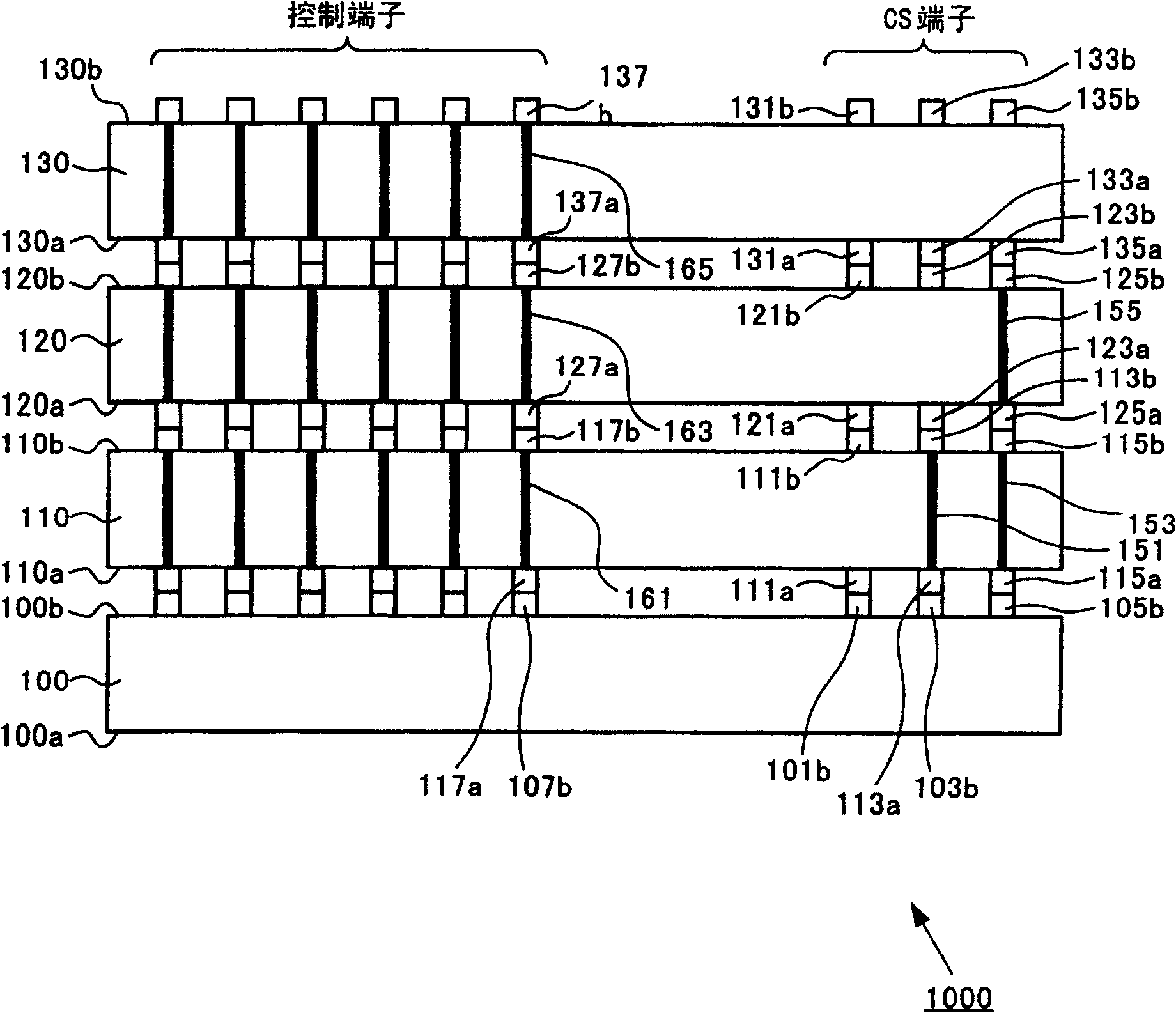
[0156] Figure 8 It is a cross-sectional configuration diagram of a lamination apparatus related to the second embodiment. In the stacking device 2000 , a master device 200 , a first slave device 210 , a second slave device 220 , a third slave device 230 , and a fourth slave device 240 are stacked. In addition, the terminals include a plurality of control terminals to which control signals for each slave device to perform various processes are input, and a plurality of CS terminals to which identification commands from the master device 200 are input. The example shown here is an example in which four slave devices are stacked, but the number of stacks is not limited.
[0157] (2) CS terminal configuration and CS terminal connection confi...
no. 3 Embodiment approach example
[0212] (summary)
[0213] A stacked device is formed by stacking a plurality of slave devices with the same terminal arrangement and a master device. Here, the master device has a command transmission mechanism for inputting a random number generation command to a terminal of an adjacent slave device to start generating a random number, and receiving random numbers generated by each slave device, and judging whether the values are different from each other. The judging mechanism of the random number, and the identification ID receiving mechanism for receiving the identification ID of each slave device set corresponding to the random number generation command from each slave device, and the correspondence for storing each slave device in correspondence with each identification ID Storage institution. In addition, the slave device has a through wiring for connecting an adjacent slave device to at least one terminal of the own device, a command receiving mechanism for receivin...
PUM
| Property | Measurement | Unit |
|---|---|---|
| Resistance | aaaaa | aaaaa |
Abstract
Description
Claims
Application Information
 - R&D
- Intellectual Property
- Life Sciences
- Materials
- Tech Scout
- Unparalleled Data Quality
- Higher Quality Content
- 60% Fewer Hallucinations
Browse by: Latest US Patents, China's latest patents, Technical Efficacy Thesaurus, Application Domain, Technology Topic, Popular Technical Reports.
© 2025 PatSnap. All rights reserved.Legal|Privacy policy|Modern Slavery Act Transparency Statement|Sitemap|About US| Contact US: help@patsnap.com