Liquid crystal display with transparent conductive film on coated formed sandwich insulation film

A liquid crystal display, transparent conductive film technology, applied in static indicators, instruments, nonlinear optics, etc., can solve problems such as total resistance change

Inactive Publication Date: 2008-11-26
NEC LCD TECH CORP
View PDF7 Cites 0 Cited by
  • Summary
  • Abstract
  • Description
  • Claims
  • Application Information

AI Technical Summary

Problems solved by technology

Therefore, the total resistance of the common wiring conductor inevitably becomes high

Method used


Image

  • Liquid crystal display with transparent conductive film on coated formed sandwich insulation film
  • Liquid crystal display with transparent conductive film on coated formed sandwich insulation film
  • Liquid crystal display with transparent conductive film on coated formed sandwich insulation film

Examples


no. 1 example

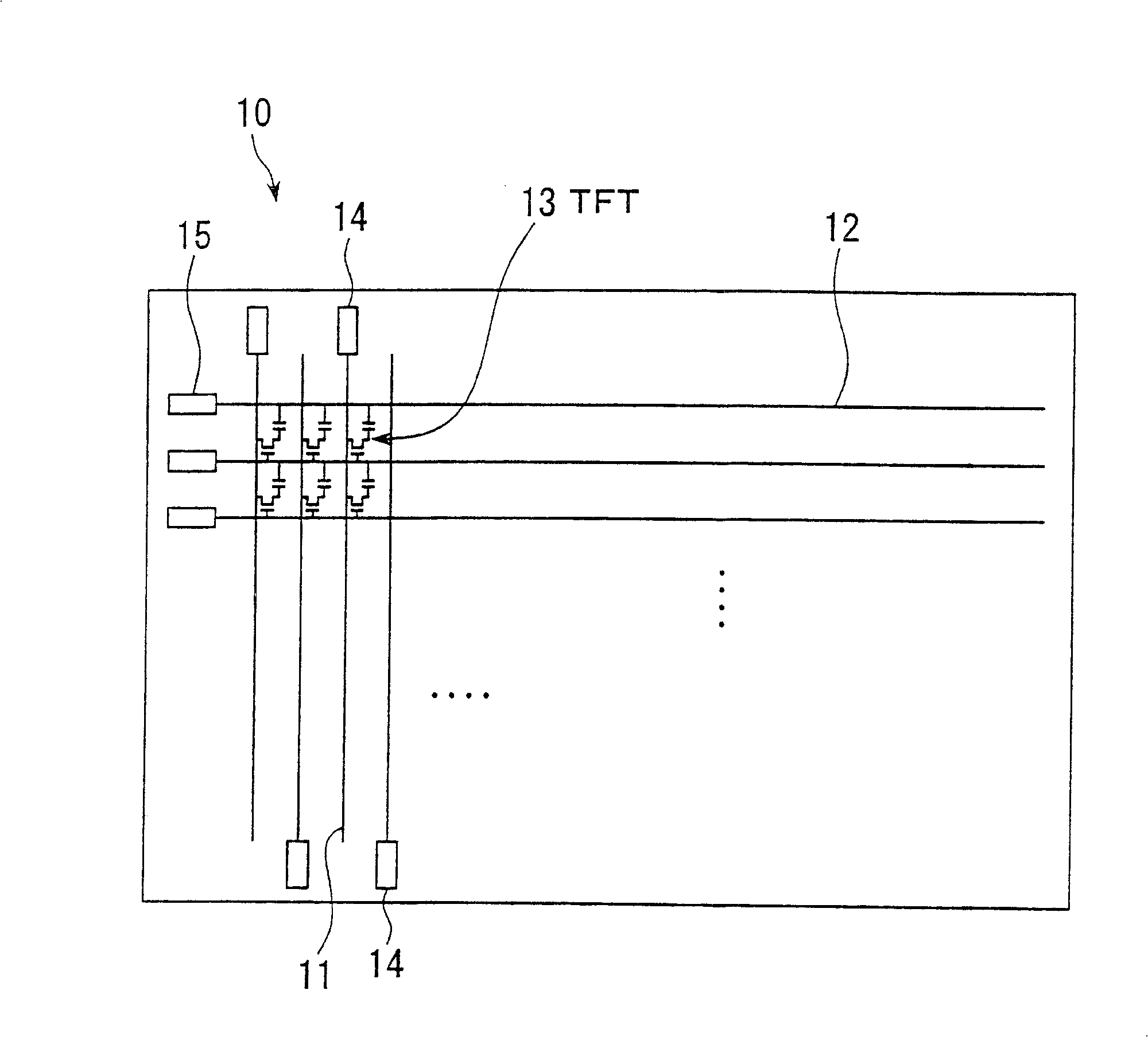
[0071] figure 1 It is a schematic plan view describing the TFT substrate structure of the transmissive liquid crystal display according to the first embodiment of the present invention. Make figure 1 The TFT substrate 10 shown in FIG. 1 and the opposing substrate 17 mentioned later face each other, and a liquid crystal material is filled in the space between the TFT substrate 10 and the opposing substrate 17 to form a liquid crystal display of a liquid crystal display. Board (see figure 2 with Figure 4 ).

[0072] On the surface of the TFT substrate 10 facing the opposite substrate 17 side, a plurality of signal lines 11 and a plurality of scanning lines 12 intersecting the signal lines 11 are provided in a grid shape. In the vicinity of each intersection of one of the signal lines 11 and one of the scanning lines 12, a TFT 13 is formed. Therefore, the TFT 13 is arranged in a matrix.

[0073] In this embodiment, the TFT13 constitutes a high-resolution liquid crystal display p...

no. 2 example

[0117] Picture 10 It is a schematic plan view describing the structure of the TFT substrate 50 in the transmissive liquid crystal display according to the second embodiment of the present invention. Such as Picture 10 As shown, on the surface of the TFT substrate 50 on the opposite substrate side not shown in the drawings, a plurality of signal lines 11 and a plurality of scanning lines 12 intersecting the signal lines 11 are arranged in a grid-like arrangement. . In the vicinity of the intersection of one of the signal lines 11 and one of the scanning lines 12, a TFT 13 is formed. Thus, the TFTs 13 are arranged in a matrix.

[0118] A common wiring conductor, that is, a common wiring 51 is also provided between adjacent scan lines 12. In the common storage type liquid crystal display, the common wiring conductor 51 and the pixel electrode form a storage capacitor.

[0119] The common wiring conductors 51 are coupled to each other, and a common potential is applied thereto. So,...


PUM

PropertyMeasurementUnit
temperatureaaaaaaaaaa
thicknessaaaaaaaaaa
thicknessaaaaaaaaaa

Abstract

One kind of LCD is made, which has lattice buses, switch elements coupled to the buses, and pixel electrodes set on coating formed insulating film and coupled to the switch elements. During making the LCD, the transparent conducting film is formed on the sandwiched insulating film at the substrate temperature controlled at 100-170 deg.c. Or, the transparent conducting film is formed on the sandwiched insulating film under the conditions of no-heating state and oxygen flow rate ratio controlled in 1 % or lower, and the formed transparent conducting film is then annealed. Therefore, when ITO film is etched on the sandwiched insulating film, no corrosive residue is generated. In addition, the contact resistance between the ITO film and the lower metal layer is reduced to avoid display fault.

Description

[0001] This application is a divisional application of the patent application named "Liquid Crystal Display with Transparent Conductive Film on the Interlayer Insulating Film Formed by Coating" and the application number is 02130565.X filed on August 16, 2002. Technical field [0002] The invention relates to a liquid crystal display and a manufacturing method thereof. More specifically, the present invention relates to a liquid crystal display having a high-resolution display panel in which an insulating film formed by coating, for example, an organic film or the like is used as an interlayer insulating film. Background technique [0003] Generally, a transparent type liquid crystal display is widely used, in which a thin film transistor (TFT) or a metal insulator insulator (MIM) device is used as a leading element for driving and controlling each pixel. [0004] Figure 22A It is a partially enlarged plan view showing the pixel portion of the active matrix substrate of the conv...

Claims


Application Information

Patent Timeline
Patent Type & Authority Patents(China)
IPC IPC(8): G02F1/1333G02F1/133
Inventor 木村茂前田明寿土居悟史石野隆行
Owner NEC LCD TECH CORP
Why Eureka
Try Eureka