
Wiring structure for coupling chip

A wiring structure and chip technology, applied in nonlinear optics, instruments, optics, etc., can solve problems such as unfavorable product miniaturization, affecting the design size of integrated circuit chips 15, increasing manufacturing costs, etc.

Active Publication Date: 2009-03-11
AU OPTRONICS CORP
View PDF5 Cites 0 Cited by
  • Summary
  • Abstract
  • Description
  • Claims
  • Application Information

AI Technical Summary

Problems solved by technology

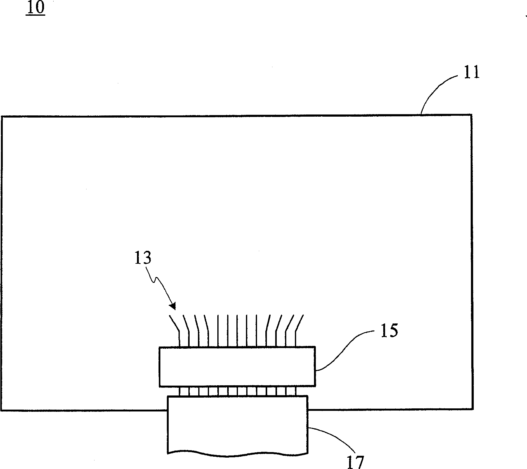
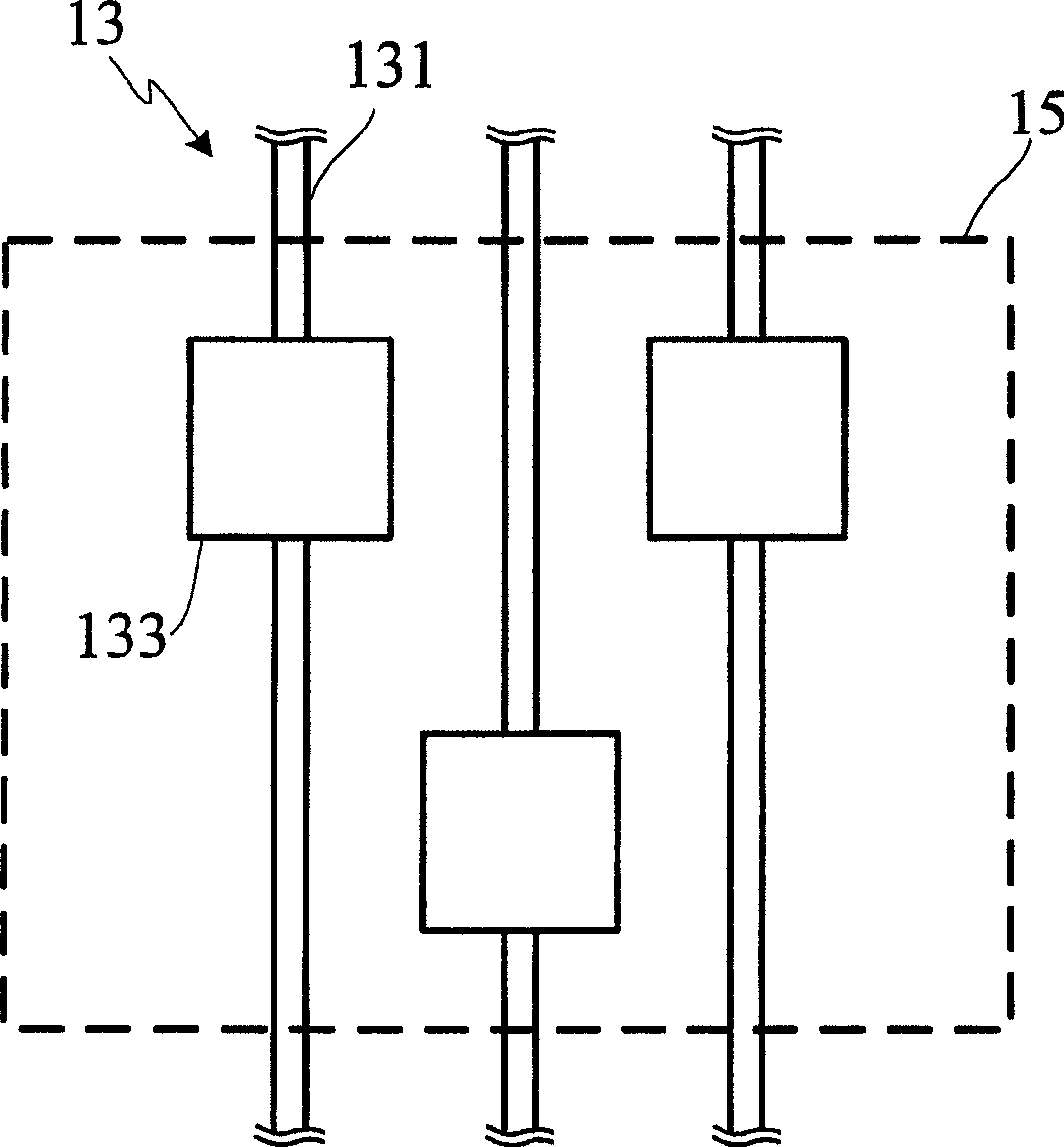
From a process point of view, in order to reduce the size, the distance between the lines 131 or between the conductive pads 133 should be as small as possible. The larger the distance between the better, these two indicators are usually contradictory and difficult to choose
In actual design and manufacturing, the distance between the conductive pad 133 and the circuit 131 will be estimated according to the machine capacity, incoming material error, and the manufacturer's self-assessed process stability standards, etc., which will also affect the design size of the integrated circuit chip 15
[0007] In the existing process, limited by the stability of the machine and its process capability, the occupied area of ​​the integrated circuit chip 15 is too large, and the display area is compressed, which is not conducive to product miniaturization
If you want to use a smaller integrated circuit chip 15, you must use a higher-precision flip-chip machine, which will increase the manufacturing cost

Method used


Image

  • Wiring structure for coupling chip
  • Wiring structure for coupling chip
  • Wiring structure for coupling chip

Examples


Embodiment Construction

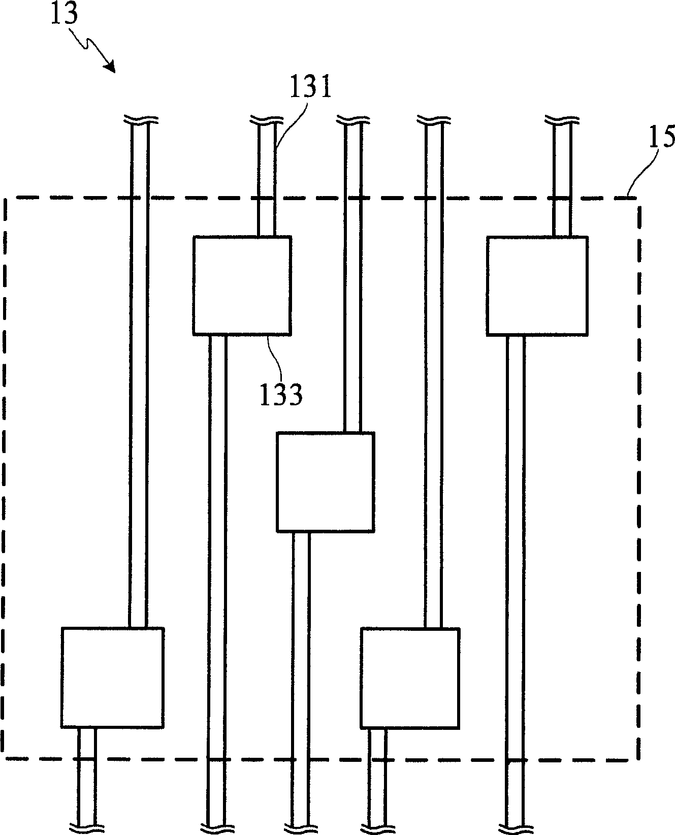
[0045] According to the present invention as image 3 In the preferred embodiment shown, the wiring structure 20 used in the present invention for coupling chips is arranged on the substrate of the liquid crystal display. For the convenience of illustration, a first direction X and a second direction Y that are substantially perpendicular to each other can be defined on the substrate. . The wiring structure 20 of the present invention includes at least one unit 30, and the unit 30 includes a plurality of lines and a plurality of conductive pads; Electrical conduction can be achieved after bonding.

[0046] Specifically, the plurality of lines includes a first line 41, a second line 42, and a third line 43, the lines are substantially parallel to each other and extend toward the second direction Y; and the plurality of conductive pads include a first conductive pad 51 . The second conductive pad 52 and the third conductive pad 53 are disposed on the first circuit 41 , the sec...


PUM

PropertyMeasurementUnit
sizeaaaaaaaaaa
sizeaaaaaaaaaa

Abstract

A wiring structure used on coupled chip consists of a unit including multiple circuit being set in parallel to each other and being extended towards the second direction, multiple conductive pad being set on said circuits separately. It is featured as arranging adjacent conductive pads in sequence on the first direction but alternatively to each other on the second direction, setting said multiple circuit in corresponding to its adjacent pads and arranging an offset unit being towards to the first direction far away from said conductive pad on multiple circuit.

Description

technical field [0001] The invention relates to a wiring structure for coupling chips, in particular to a wiring structure which can ensure electrical conduction with the chip under the precision of existing machines, thereby reducing the size of the chip. Background technique [0002] Due to the advantages of power saving, light weight, low radiation and easy portability, liquid crystal displays (Liquid Crystal Displays, LCDs) have gradually replaced traditional displays and become the mainstream of the display market. Among them, in addition to key components such as backlight modules, liquid crystals, and color filters, liquid crystal displays also convert external signals into control signals through integrated circuit chips and wiring structures on the panel, and then determine the brightness of each pixel. [0003] Known liquid crystal display 10 such as figure 1 As shown, a wiring structure 13 is formed on the glass substrate 11, and at the lowermost edge of the glas...

Claims


Application Information

Patent Timeline
Patent Type & Authority Patents(China)
IPC IPC(8): G02F1/1345G02F1/1362G02F1/133
Inventor 林绍平洪硕彦
Owner AU OPTRONICS CORP
Learn More