Bridging multi-chip packaging structure

A multi-chip packaging and chip technology, applied in electrical components, electrical solid devices, circuits, etc., can solve the problems of poor characteristic impedance matching, signal attenuation, poor power supply and grounding effect, etc. Signal attenuation, to avoid the effect of impedance mismatch

Inactive Publication Date: 2009-04-01
ADVANCED SEMICON ENG INC
View PDF6 Cites 0 Cited by
  • Summary
  • Abstract
  • Description
  • Claims
  • Application Information

AI Technical Summary

Problems solved by technology

[0004] In the above-mentioned packaging structure, the first chip 12 is electrically connected to the second chip 14 through the wire 164. However, because the cross-sectional area of ​​the wire 164 is very small and the length is very long, the characteristic impedance matching is poor, so that the signal will be rapidly attenuated. , and when high-frequency circuits are operating, there will be inductance and capacitance parasitic effects (Parasitics), resulting in signal reflections
In addition, due to the very small area of ​​the transmission path between the wire 164 and the first chip contact, it is not conducive to the supply of voltage and current, resulting in poor power and grounding effects.

Method used


Image

  • Bridging multi-chip packaging structure
  • Bridging multi-chip packaging structure
  • Bridging multi-chip packaging structure

Examples


Embodiment Construction

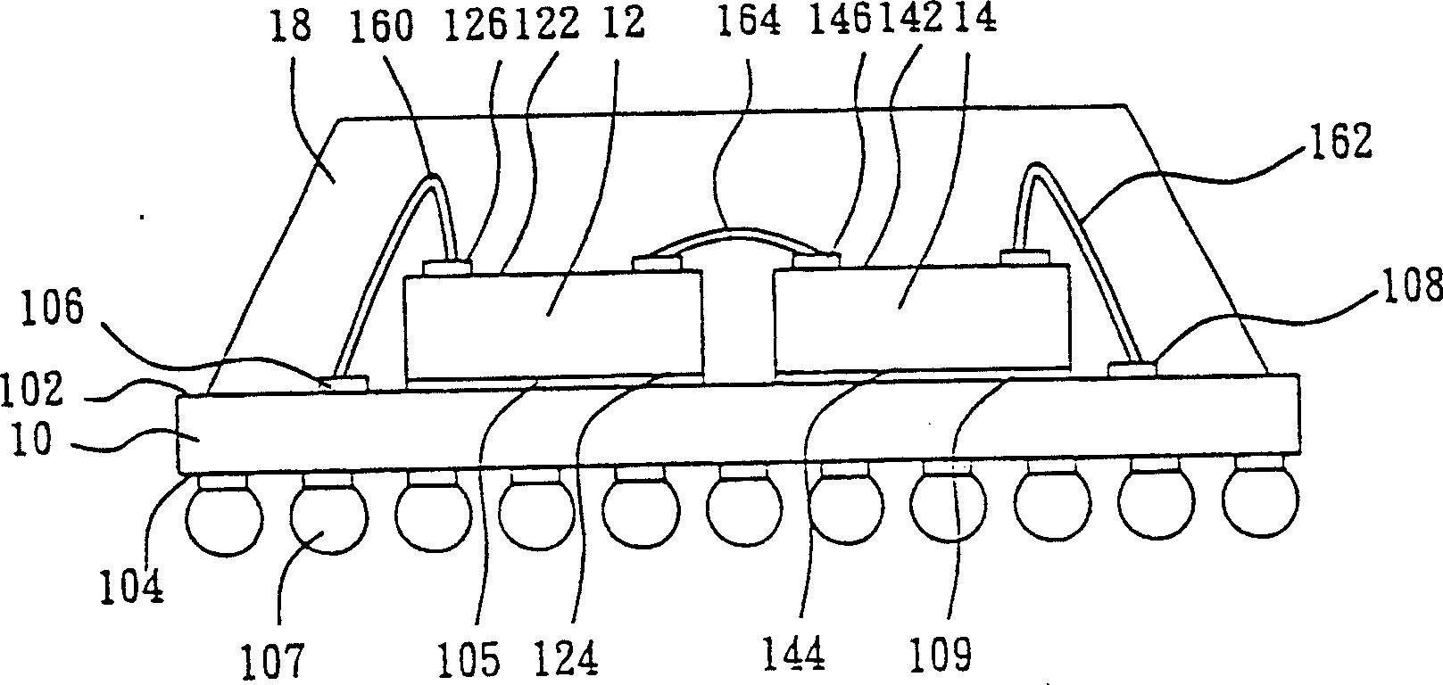
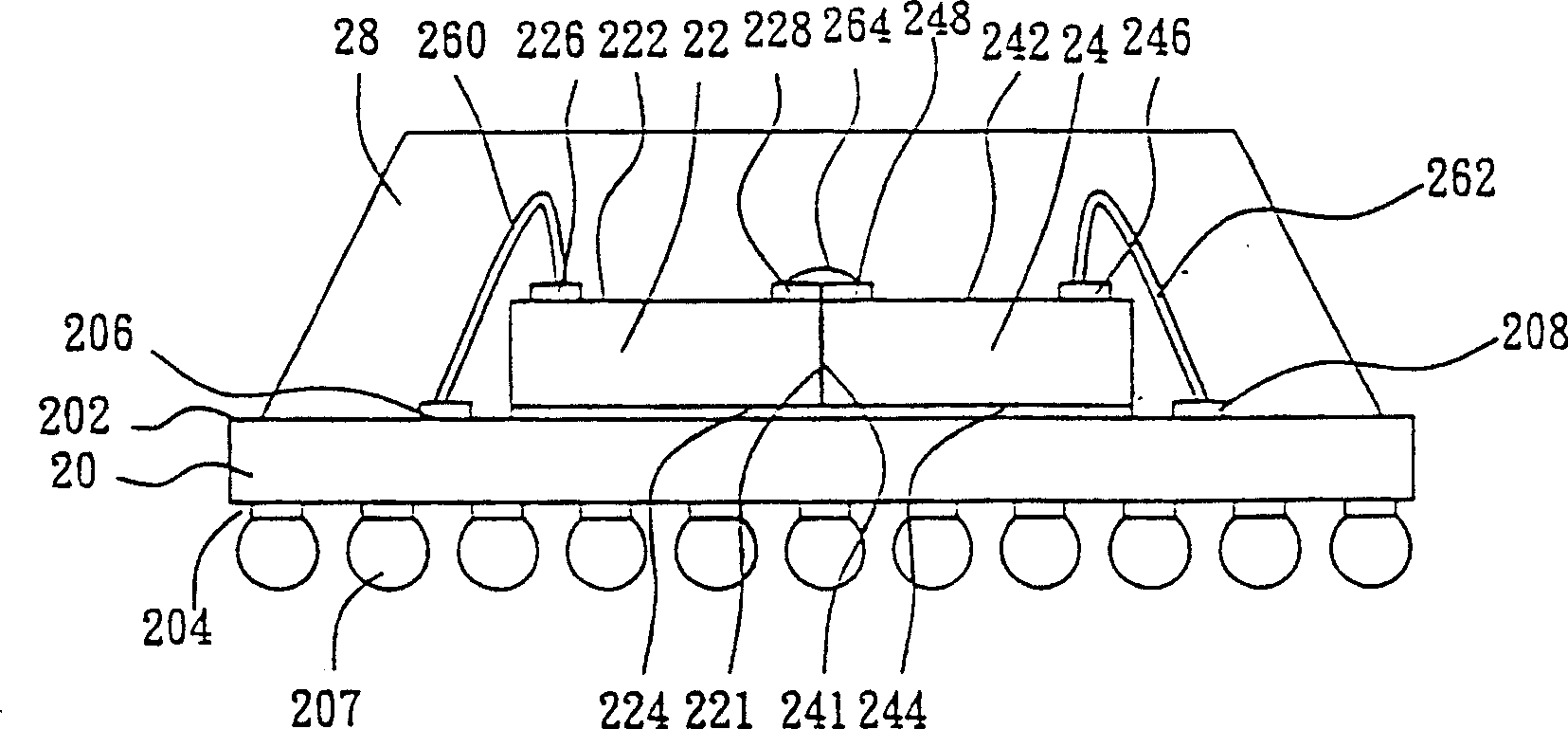
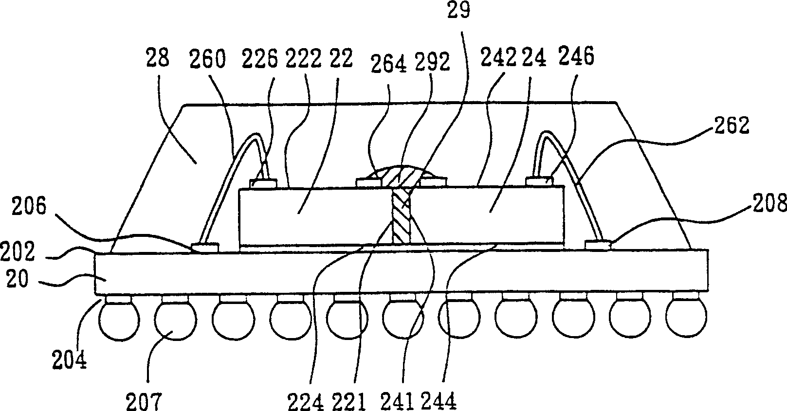
[0066] figure 2 A bridged multi-chip package structure according to the first preferred embodiment of the present invention is disclosed, which mainly includes a carrier 20 , a first chip 22 , a second chip 24 and a conductive bump 264 . The carrier board 20 has an upper surface 202 and a corresponding lower surface 204 , and a plurality of carrier board contacts 206 , 208 are located on the upper surface of the carrier board 20 . The first chip 22 has a first active surface 222 , and the first chip 22 also has at least one first contact 226 disposed on the first active surface 222 of the first chip 22 . Likewise, the second chip 24 has a second active surface 242 , and the second chip 24 also has at least one second contact 246 disposed on the second active surface 242 of the second chip 24 . Wherein, the first chip 22 is arranged on the carrier 20 with its back side (the first back side 224) and through an adhesive material (such as silver glue); An adhesive material (suc...


PUM


Abstract

The present invention relates to a bridged type multi-chip package structure. It mainly includes a carrier plate, a first chip, a second chip and at least a conductive body. Said carrier plate has an upper surface and correspondent lower surface, several carrier plate contacts are positioned on upper surface of said carrier plate. The first chip has a first active surface, said first chip also has at least a first contact which is placed on first active surface of said first chip. Similarly, the second chip has a second active surface, said second active surface also has at least a second contact. Which is placed on second active surface of said second chip. The first side wall of first chip is adjacent to second side wall of second chip, and the first active surface of first chip and second active surface of second chip are placed on a common plane. The conductive body is extended on first active surface of first chip and second active surface of second chip so as to make first contact of first chip and second contact of second chip be electrically connected.

Description

technical field [0001] The invention relates to a multi-chip packaging structure, in particular to a bridge-type multi-chip packaging structure. Background technique [0002] In recent years, with the rapid development of electronic technology, high-tech electronic products have also come out one after another, so more humanized and functional electronic products are constantly being introduced. However, all kinds of products are designed towards the trend of light, thin, short and small. To provide more convenient and comfortable use. In the completion of an electronic product, electronic packaging plays an important role. There are generally two ways of electrical connection between chips. The first is wire-bonding, and the second is wire-bonding. Flip chip (flip chip) way. As far as the wire bonding method is concerned, it uses a wire bonding machine to move its wire bonding head to the contact point of the chip first, and uses tip discharge to melt the ends of the cond...

Claims


Application Information

Patent Timeline
Patent Type & Authority Patents(China)
IPC IPC(8): H01L25/04H01L23/12H01L23/48H01L23/34
CPCH01L24/73H01L2224/24137H01L2224/48091H01L2224/48137H01L2224/48227H01L2224/73265H01L2924/15311H01L2924/18165H01L2924/181H01L2924/00014H01L2924/00012
Inventor 洪志斌
Owner ADVANCED SEMICON ENG INC
Why Eureka
Try Eureka