Supercharge Your Innovation With Domain-Expert AI Agents!

Capacitor with nona-composite dielectric medium structure and method for manufacturing the same

A nanocomposite, dielectric technology, applied in capacitors, semiconductor/solid-state device manufacturing, nanotechnology, etc., can solve problems such as difficulty in ensuring high dielectric constant HfAlO nanocomposite dielectric layers

Inactive Publication Date: 2009-04-22
SK HYNIX INC
View PDF4 Cites 0 Cited by
  • Summary
  • Abstract
  • Description
  • Claims
  • Application Information

AI Technical Summary

Problems solved by technology

As a result, it may be difficult to guarantee the expected high-k dielectric constant HfAlO nanocomposite dielectric layer in sub-80nm devices

Method used


Image

  • Capacitor with nona-composite dielectric medium structure and method for manufacturing the same
  • Capacitor with nona-composite dielectric medium structure and method for manufacturing the same
  • Capacitor with nona-composite dielectric medium structure and method for manufacturing the same

Examples


Embodiment Construction

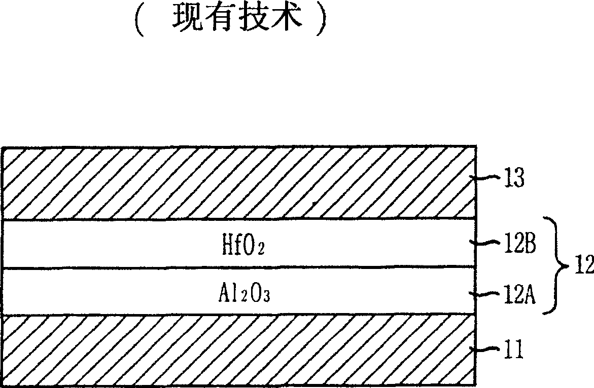
[0031] Hereinafter, a capacitor having a nanocomposite dielectric structure and a method of manufacturing the same according to exemplary embodiments of the present invention will be described in detail with reference to the accompanying drawings.

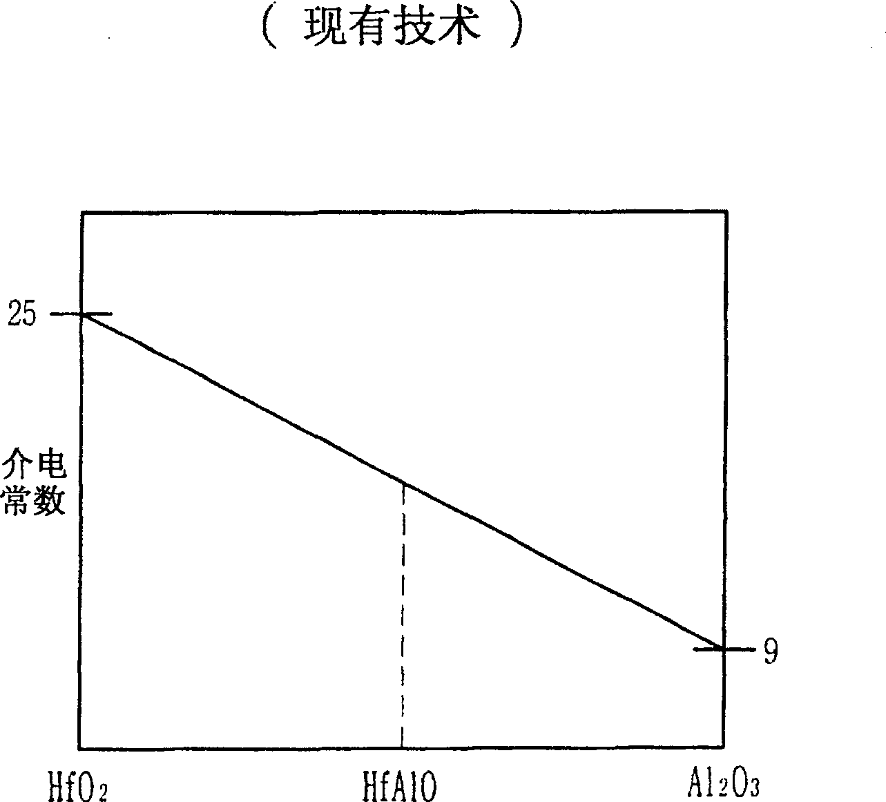
[0032] Exemplary embodiments of the present invention propose a dielectric structure with Al 2 o 3The same good leakage current characteristics can guarantee greater than about 20, close to HfO 2 The high dielectric constant of the dielectric constant, and can be applied to various types of capacitors. These advantages make it possible to apply the dielectric layer to highly integrated semiconductor devices having dimensions smaller than about 70 nm.

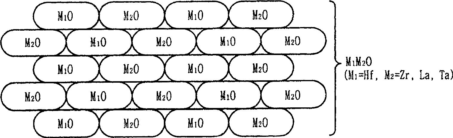
[0033] image 3 is a diagram depicting the concept of a nanocomposite dielectric structure according to an embodiment of the present invention. According to a specific embodiment of the present invention, the nanocomposite dielectric structure is not a simple stacked structure of...


PUM


Abstract

It provides a capacitor of nanocomposite dielectric structure and manufacturing method. This capacitor include: down-electrode, nanocomposite dielectric structure and up-electrode. The nanocomposite dielectric structure is achieved by mixing the layer of hafnium oxide (HfO2) and dielectric which dielectric constant is equal to or greater than layer's dielectric constant of HfO2. The dielectric layer include materials of ZrO2, La2O3 and Ta2O5,and each layer has a dielectric constant about 25 to about 30 and a band-gap energy level about 4.3 to 7.8.

Description

technical field [0001] The present invention relates to semiconductor devices and methods of manufacturing the same; and more particularly, to capacitors having nanocomposite dielectric structures and methods of manufacturing the same. Background technique [0002] Since the large-scale integration of memory products has been accelerated by miniaturization in semiconductor technology, the size of unit cells has rapidly shrunk and low operating voltages can be realized. However, despite the reduced cell size, the capacity required to operate a memory device should be greater than 25pF per cell to prevent soft error events and reduce refresh times. Therefore, even though a three-dimensional storage node having a hemispherical electrode surface with a large surface area has been realized, for using silicon nitride (Si 3 N 4 ) layer of dynamic random access memory (DRAM) NO capacitor height has continued to increase. The silicon nitride layer is typically formed using dichlor...

Claims


Application Information

Patent Timeline
Patent Type & Authority Patents(China)
IPC IPC(8): H01L27/108H01L27/102H01L27/10H01L21/8242H01L21/8222H01L21/82H01L21/02H01L21/31H01B3/10
CPCC23C16/45531H01L27/1085B82Y10/00H01L21/3142H01L28/40C23C16/405H01L21/02183H01L21/02192H01L21/02189H01L21/0217H01L21/0228H01L21/02181H01L21/02255H10B12/03A47G9/10
Inventor 吉德信洪权
Owner SK HYNIX INC
Features
  • R&D
  • Intellectual Property
  • Life Sciences
  • Materials
  • Tech Scout
  • Unparalleled Data Quality
  • Higher Quality Content
  • 60% Fewer Hallucinations
Learn More