Amplified solid-state image pickup device
A solid-state imaging device and pixel technology, which is applied in electric solid-state devices, semiconductor devices, image communication, etc., can solve problems such as the influence of afterimage characteristics, the inability to fully read signal charges, and the deterioration of signal linearity
- Summary
- Abstract
- Description
- Claims
- Application Information
AI Technical Summary
Problems solved by technology
Method used
Image
Examples
Embodiment approach 1
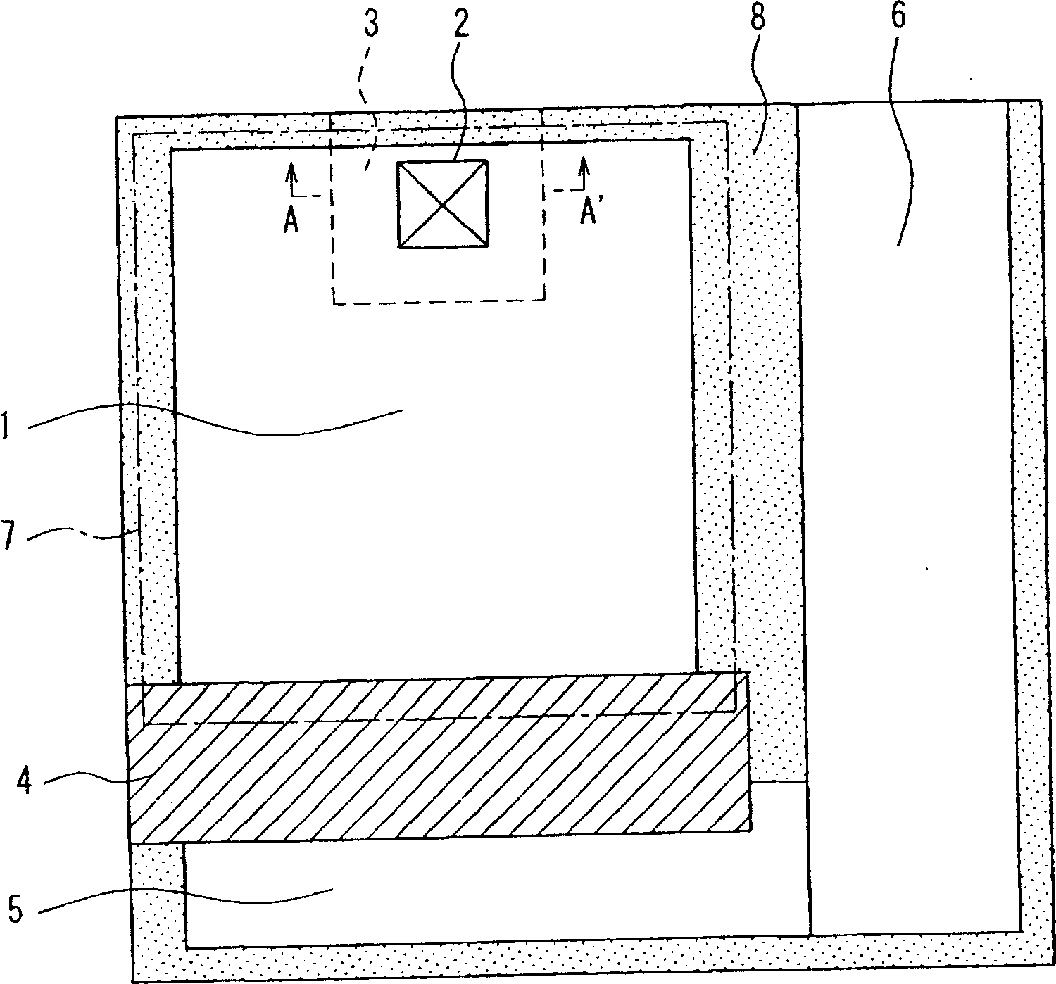
[0069] figure 1 is a schematic plan view showing a pixel portion of the amplified solid-state imaging device according to the first embodiment. The layout of this device is roughly divided into a photodiode section 1 , a floating diffusion capacitance section 5 , and a transistor arrangement section 6 . Transistors (not shown), such as reset transistors, drive transistors, and selection transistors, are arranged in the transistor arrangement unit 6 . A signal charge transfer gate 4 is provided between the photodiode unit 1 and the floating diffusion capacitor unit 5. 7 denotes a light-shielding aluminum opening. 8 indicates an inactive area.
[0070] The signal charge photoelectrically converted and stored in the photodiode unit 1 is transferred to the floating diffusion capacitor unit 5 through the signal charge transfer gate 4 . The signal charge is converted into a voltage by the floating diffusion capacitance section 5 , and amplified or impedance converted by the driv...
Embodiment approach 2
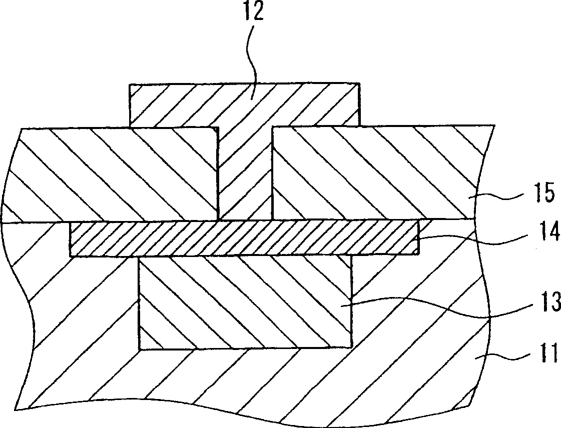
[0080] Constructed with reference to the cross-section representing the GND contact within the pixel figure 2 , the amplified solid-state imaging device of Embodiment 2 will be described.
[0081] A first conductivity type well region 13 and a first conductivity type surface layer 14 are formed in the second conductivity type photodiode injection region 11 . An in-pixel GND contact 12 is provided through an insulating layer 15 and is connected to the surface layer 14 of the first conductivity type.
[0082] The present embodiment is characterized in that the first conductivity type surface layer 14 is also used instead of the contact injection portion for the connection between the in-pixel GND contact 12 and the first conductivity type well region 13 . The impurity concentration of the first conductivity type surface layer 14 is set to 1.0×10 13 ~1.0×10 15 . Usually the first conductivity type injection area used in the contact injection part is set to 1.0×10 13 ~1.0×10...
Embodiment approach 3
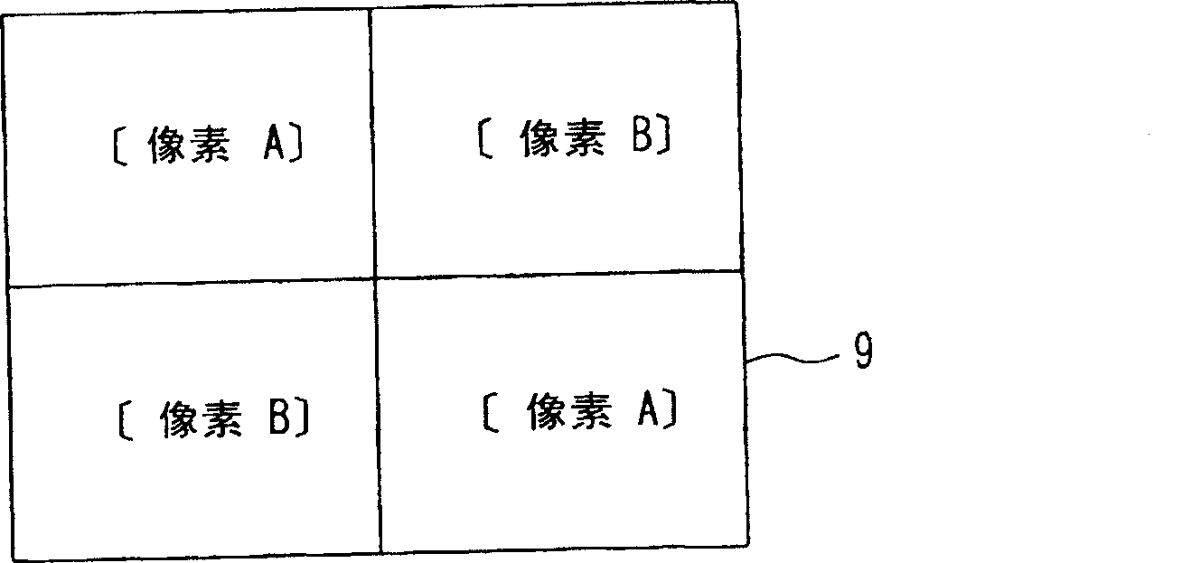
[0084] reference to the pixel layout Figure 3A-3C , the amplified solid-state imaging device of Embodiment 3 will be described. Figure 3A It is a plan view schematically showing an imaging area (only four pixels are shown) 9 . Should Figure 3B , 3C are floor plans representing the layout within pixels, respectively.
[0085] The present embodiment is characterized in that two or more types of pixels having different GND contact positions within the pixel are arranged in the imaging area 9 . That is, in the pixel A, the in-pixel GND contact 2 a and the first conductivity type well region 3 a are arranged on the upper right side of the photodiode 1 . In the pixel B, the in-pixel GND contact 2 b and the first conductivity type well region 3 b are arranged on the upper left side of the photodiode 1 . Such as Figure 3A As shown, pixels A are arranged on the upper left and lower right in the imaging area 9, and pixels B are arranged on the lower left and upper right.
[0...
PUM
 Abstract
Description
Claims
Application Information
 - R&D
- Intellectual Property
- Life Sciences
- Materials
- Tech Scout
- Unparalleled Data Quality
- Higher Quality Content
- 60% Fewer Hallucinations
Browse by: Latest US Patents, China's latest patents, Technical Efficacy Thesaurus, Application Domain, Technology Topic, Popular Technical Reports.
© 2025 PatSnap. All rights reserved.Legal|Privacy policy|Modern Slavery Act Transparency Statement|Sitemap|About US| Contact US: help@patsnap.com


