Amplified solid-state image pickup device
A technology for solid-state imaging devices and pixels, which is applied in the direction of electric solid-state devices, semiconductor devices, electrical components, etc., can solve problems such as the reduction of the transfer gate 44, the influence of afterimage characteristics, and the inability to fully read signal charges.
- Summary
- Abstract
- Description
- Claims
- Application Information
AI Technical Summary
Problems solved by technology
Method used
Image

Examples
Embodiment approach 1
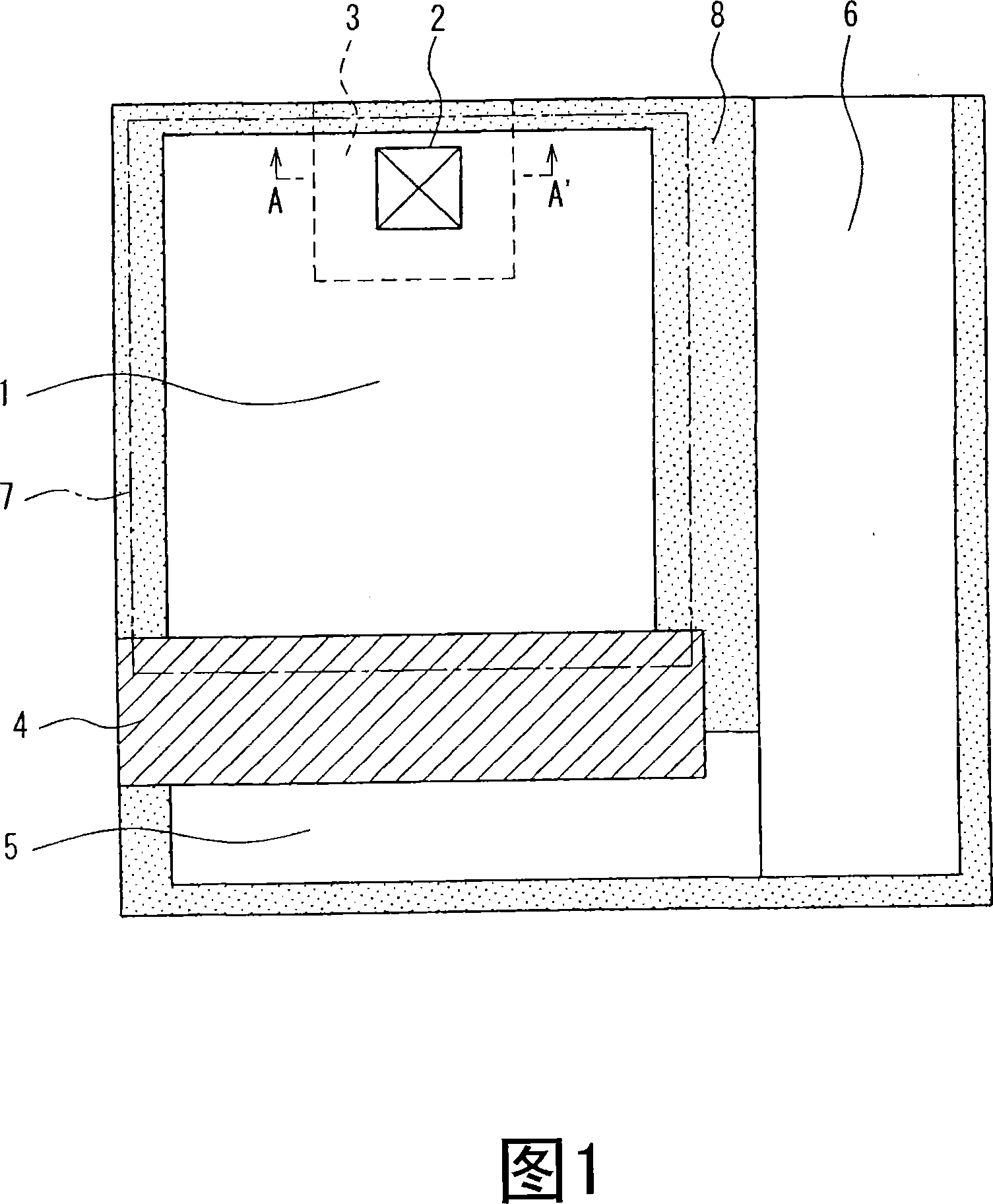
[0069]FIG. 1 is a schematic plan view showing a pixel portion of an amplified solid-state imaging device according to Embodiment 1. FIG. The layout of this device is roughly divided into a photodiode section 1 , a floating diffusion capacitance section 5 , and a transistor arrangement section 6 . Transistors (not shown), such as reset transistors, drive transistors, and selection transistors, are arranged in the transistor arrangement unit 6 . A signal charge transfer gate 4 is provided between the photodiode unit 1 and the floating diffusion capacitor unit 5. 7 denotes a light-shielding aluminum opening. 8 indicates an inactive area.
[0070] The signal charge photoelectrically converted and stored in the photodiode unit 1 is transferred to the floating diffusion capacitor unit 5 through the signal charge transfer gate 4 . The signal charge is converted into a voltage by the floating diffusion capacitance section 5 , and amplified or impedance converted by the driving trans...
Embodiment approach 2
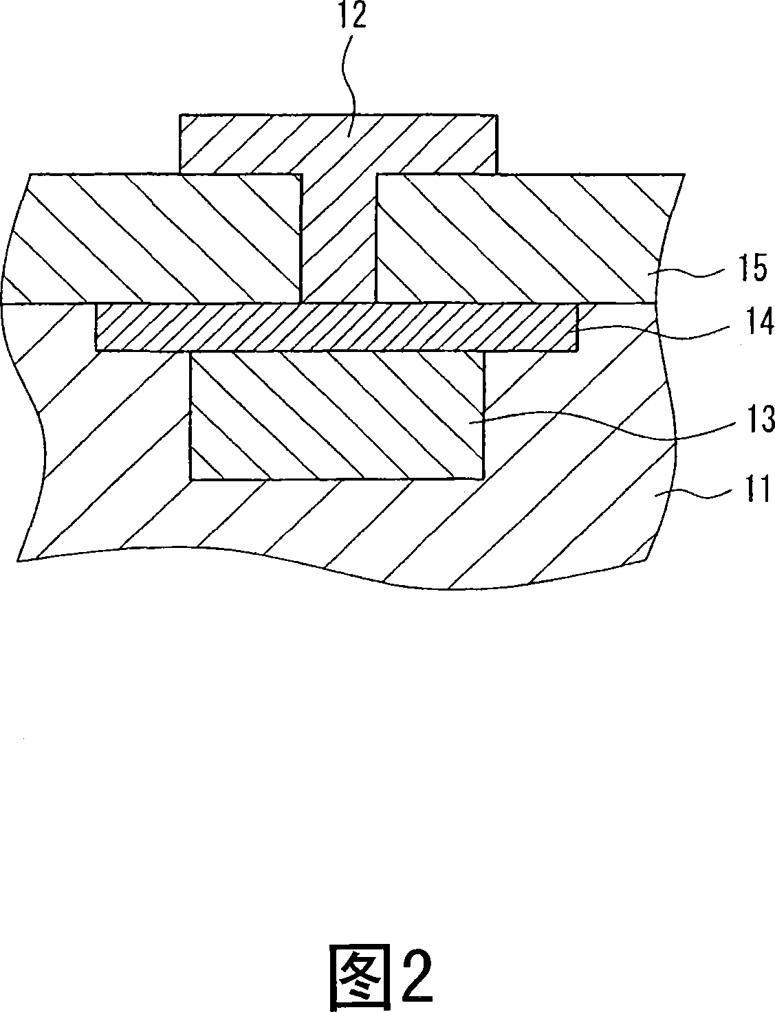
[0080] An amplifying solid-state imaging device according to Embodiment 2 will be described with reference to FIG. 2 showing a cross-sectional structure of a GND contact in a pixel.
[0081] A first conductivity type well region 13 and a first conductivity type surface layer 14 are formed in the second conductivity type photodiode injection region 11 . An in-pixel GND contact 12 is provided through an insulating layer 15 and is connected to the surface layer 14 of the first conductivity type.
[0082] The present embodiment is characterized in that the first conductivity type surface layer 14 is also used instead of the contact injection portion for the connection between the in-pixel GND contact 12 and the first conductivity type well region 13 . The impurity concentration of the first conductivity type surface layer 14 is set to 1.0×10 13 ~1.0×10 15 . Usually the first conductivity type injection area used in the contact injection part is set to 1.0×10 13 ~1.0×10 14 , s...
Embodiment approach 3
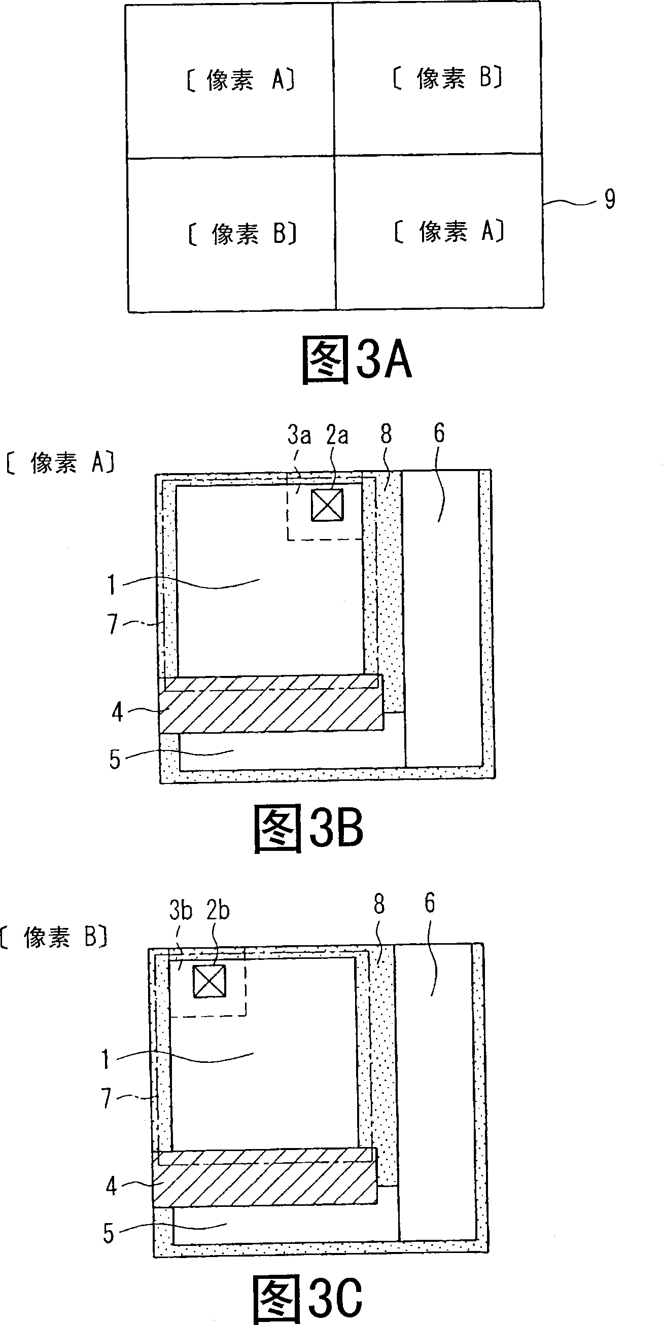
[0084] An amplified solid-state imaging device according to Embodiment 3 will be described with reference to FIGS. 3A to 3C showing pixel layouts. FIG. 3A is a plan view schematically showing an imaging area (only four pixels are shown) 9 . 3B and 3C are plan views each showing the layout in a pixel.
[0085] The present embodiment is characterized in that two or more types of pixels having different GND contact positions within the pixel are arranged in the imaging area 9 . That is, in the pixel A, the in-pixel GND contact 2 a and the first conductivity type well region 3 a are arranged on the upper right side of the photodiode 1 . In the pixel B, the in-pixel GND contact 2 b and the first conductivity type well region 3 b are arranged on the upper left side of the photodiode 1 . As shown in FIG. 3A , pixels A are arranged on the upper left and lower right in the imaging area 9 , and pixels B are arranged on the lower left and upper right.
[0086] The light incident on ea...
PUM
 Abstract
Description
Claims
Application Information
 - R&D
- Intellectual Property
- Life Sciences
- Materials
- Tech Scout
- Unparalleled Data Quality
- Higher Quality Content
- 60% Fewer Hallucinations
Browse by: Latest US Patents, China's latest patents, Technical Efficacy Thesaurus, Application Domain, Technology Topic, Popular Technical Reports.
© 2025 PatSnap. All rights reserved.Legal|Privacy policy|Modern Slavery Act Transparency Statement|Sitemap|About US| Contact US: help@patsnap.com