Pixel circuit, display device and driving method

A technology of a pixel circuit and a display device, applied in the field of pixel circuits, can solve problems such as difficulty in realizing large and high-precision display

Active Publication Date: 2009-05-13
SONY CORP
View PDF8 Cites 0 Cited by
  • Summary
  • Abstract
  • Description
  • Claims
  • Application Information

AI Technical Summary

Problems solved by technology

The former has problems such as difficulty in realizing large-scale and high-definition displays due to its simple structure, and active matrix methods are currently being actively developed.

Method used


Image

  • Pixel circuit, display device and driving method
  • Pixel circuit, display device and driving method
  • Pixel circuit, display device and driving method

Examples


Embodiment Construction

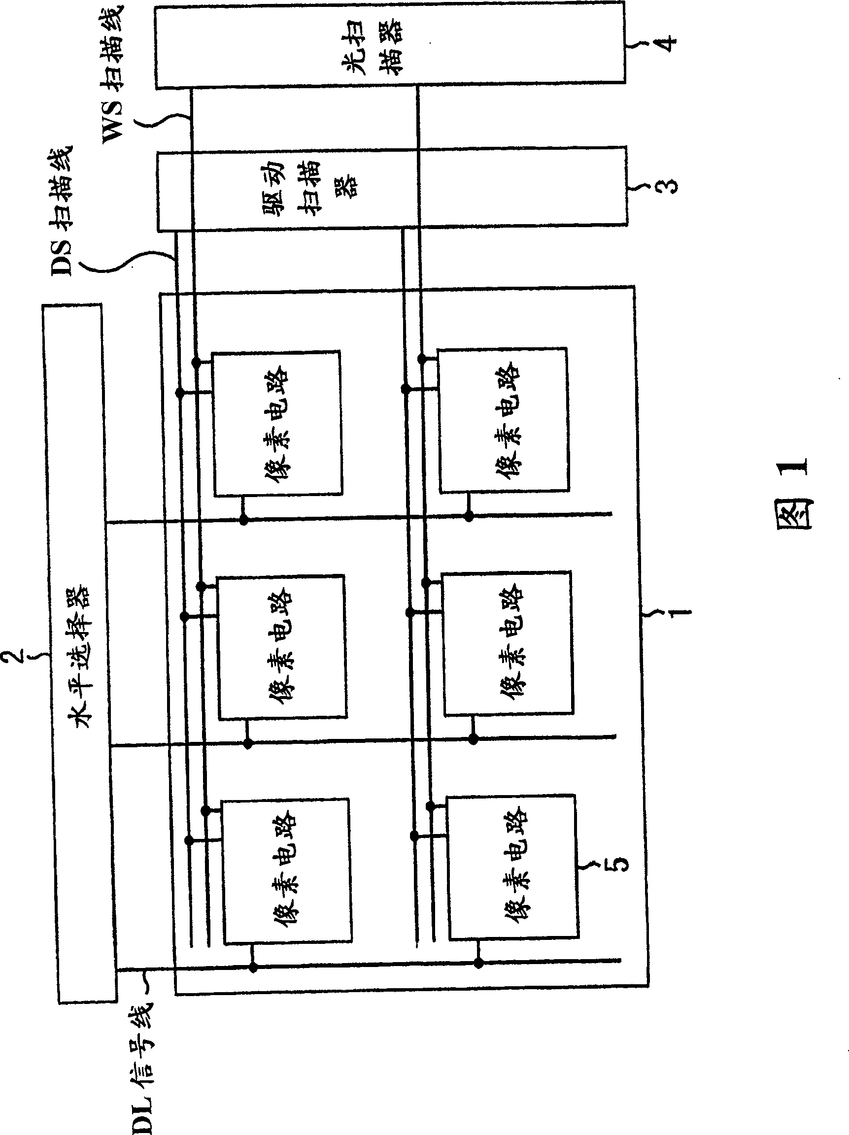
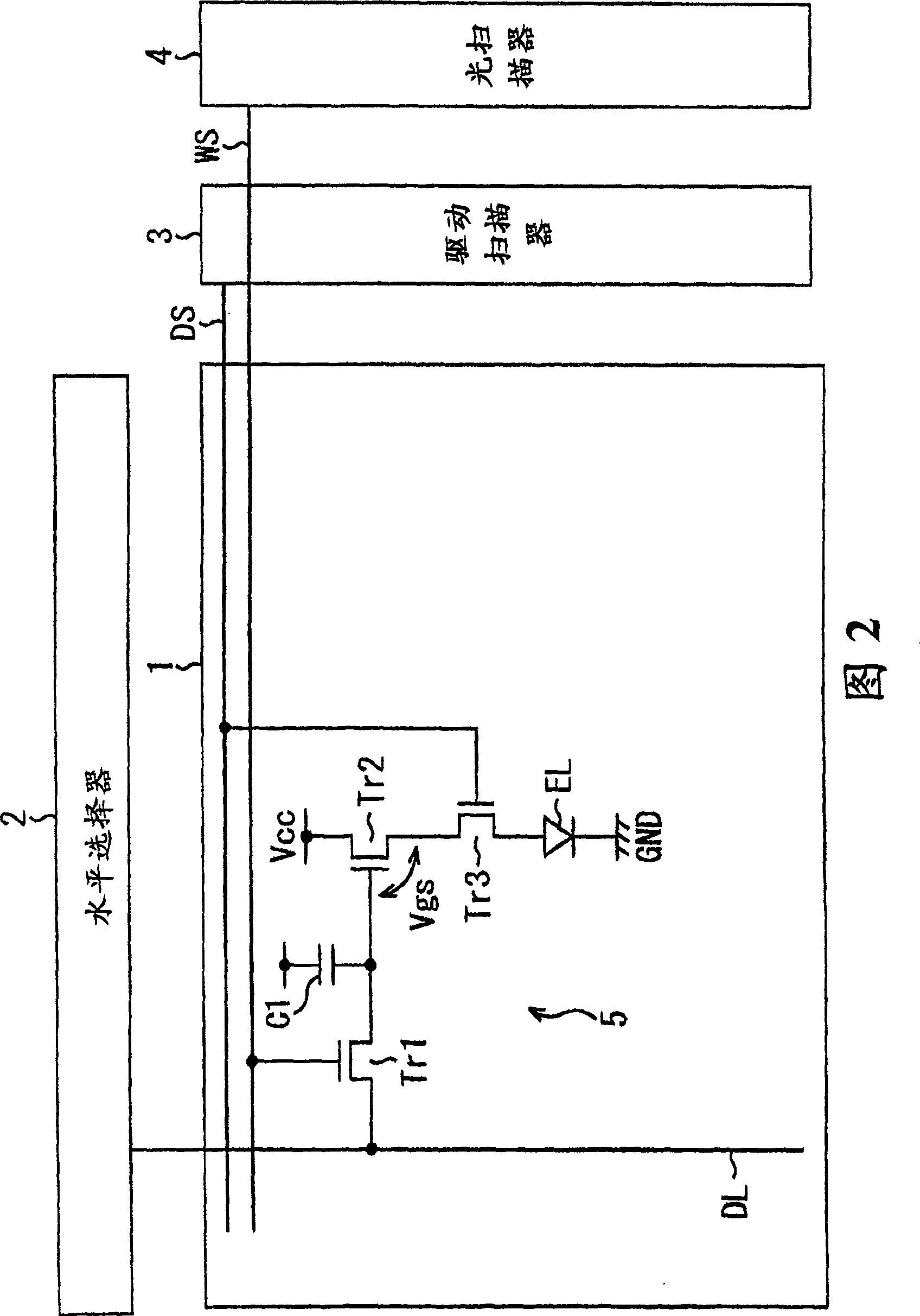
[0055] Hereinafter, embodiments of the present invention will be described in detail with reference to the drawings. First, in order to clarify the background of the present invention, a general structure of an active matrix display device and a pixel circuit contained therein will be described as a reference example with reference to FIG. 1 . As shown in the figure, the active matrix display device is composed of a pixel array 1 as a main part and peripheral circuit groups. The peripheral circuit group includes a horizontal selection selector 2, a drive scanner 3, an optical scanner 4, and the like.

[0056]The pixel array 1 is composed of row-like scanning lines WS, column-like signal lines DL, and pixel circuits 5 arranged in a matrix at the intersections of the two. The signal line DL is driven by the horizontal selector 2 . The scanning line WS is scanned by the light scanner 4 . In addition, another scanning line DS parallel to the scanning line WS is also provided, a...


PUM


Abstract

PROBLEM TO BE SOLVED: To provide a pixel circuit which compensates change with time of a drain current in a drive transistor.SOLUTION: In a drive transistor Tr2, a gate G is connected to an input node A, a source S is connected to an output node B, and a drain is connected to a power supply voltage Vcc. A sampling transistor Tr1 is connected between the input node A and a signal line DL. A holding capacitance C1 is connected to the input node A. The sampling transistor Tr1 samples an input signal Vsig from the signal line DL and holds in the holding capacitance C1. The drive transistor Tr2 supplies a drive current Ids to a light emitting element EL in accordance with the signal voltage held by the holding capacitance C1. The pixel circuit is equipped with a compensation circuit 7 to compensate a decrease in the drive current Ids caused by changes in the drive transistor Tr2 with time. The compensation circuit 7 detects a decrease in the drive current Ids through the output node B side and feedbacks the detection result to the input node A side.

Description

technical field [0001] The present invention relates to a pixel circuit for current-driving a load element arranged on each pixel. In addition, this pixel circuit is a display device arranged in a matrix, and in particular relates to a so-called active matrix system in which the amount of current passed to a load element such as an organic EL light-emitting element is controlled by an insulated gate field effect transistor provided in each pixel circuit. type of display device. Background technique [0002] In an image display device such as a liquid crystal display, an image is displayed by arranging a plurality of liquid crystal pixels in a matrix and controlling the transmission intensity or reflection intensity of incident light for each pixel according to image information to be displayed. Here, the same is true in an organic EL display using an organic EL element as a pixel, and the organic EL element is a self-luminous element, which is different from a liquid crysta...

Claims


Application Information

Patent Timeline
Patent Type & Authority Patents(China)
IPC IPC(8): G09G3/30G09G3/20H05B33/08H05B44/00
CPCY02B20/42
Inventor 内野胜秀山下淳一
Owner SONY CORP
Why Eureka
Try Eureka