Method for making floating gate discharging sharp angle

A manufacturing method and floating gate technology, which is applied in semiconductor/solid-state device manufacturing, circuits, electrical components, etc., can solve problems such as differences between chips, and achieve the effects of improving morphology, stabilizing erasing performance, and improving sharp corner morphology

Active Publication Date: 2009-05-20
SHANGHAI HUAHONG GRACE SEMICON MFG CORP +1
View PDF5 Cites 0 Cited by
  • Summary
  • Abstract
  • Description
  • Claims
  • Application Information

AI Technical Summary

Problems solved by technology

[0015] d. There will still be differences between different batches of products, resulting in differences between chips;

Method used


Image

  • Method for making floating gate discharging sharp angle
  • Method for making floating gate discharging sharp angle
  • Method for making floating gate discharging sharp angle

Examples


Embodiment Construction

[0026] The present invention will be described in further detail below in conjunction with the accompanying drawings and embodiments.

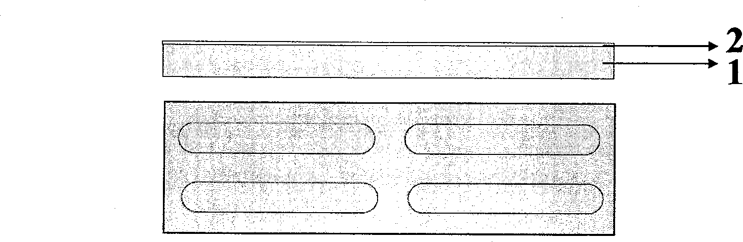
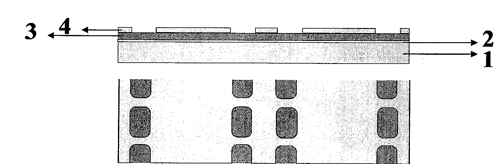
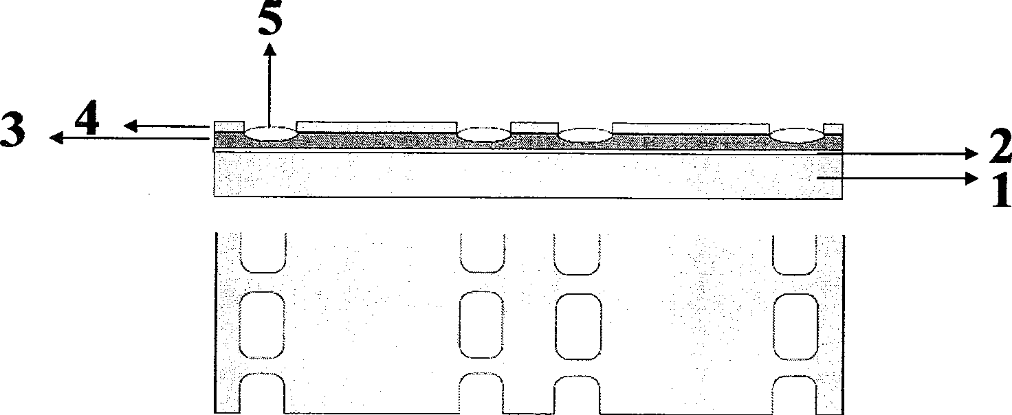
[0027] The invention provides a method for manufacturing floating gate discharge peaks, comprising the following steps: step 1, growing a layer of oxide layer on a silicon substrate to isolate the floating gate; step 2, depositing a layer of floating gate on the oxide layer Gate polysilicon; step 3, deposit a layer of SiO on the floating gate polysilicon x N y As a buffer layer when it is partially oxidized; step 4, deposit a layer of silicon nitride as a hard mask when etching the floating gate; step 5, use a photolithography to process silicon nitride and SiO x N y Etching is carried out, and the partially exposed floating gate is subjected to high-temperature thermal oxygen; step 6, the silicon nitride and SiO that have not been opened by the previous photolithography x N y and the floating gate polysilicon are etched to form floating g...


PUM


Abstract

The invention discloses a method of manufacturing a floating boom discharge sharp corner. The method comprises the steps of firstly utilizing SiH4, N2O and H2 as reaction gas and generating a layer of a SiOxNy buffer layer by the low pressure chemical vapor deposition method before silicon nitride sediment, as the buffer layer for later floating boom oxidization; in forming beak, adjusting by control technology to facilitate oxygen atoms to spread transversely toward a lateral wall underlay with certain amount. The transverse size is extended and the erasing sharp corner formed finally has a transverse extension on the upper edge, which is good for resisting the influence of subsequent floating boom etching size change on the shape of the sharp corner, improving the whole erasing performance and increasing the device stability and reliability.

Description

technical field [0001] The invention relates to a semiconductor manufacturing process, in particular to a method for manufacturing floating gate discharge sharp corners. Background technique [0002] The main features of SST (super fast) type Flash (flash memory) are: erasing (erase) is realized through the oxide film tunneling effect between the control gate and the floating gate; writing (program) is realized through channel hot electron injection. [0003] Flash memory, which is mainly used in SST IP (Super Fast IP), as a main non-volatile memory, has a wide range of uses in smart cards, microcontrollers and other fields. Compared with EEPORM, another non-volatile memory, flash memory has obvious advantages in area; but at the same time, the reliability of flash memory, especially the erasable number of times, is worse than EEPROM, so it is used in bank cards, ID cards, etc. Product has not yet been used. In the SSTIP manufacturing process, whether the erase tip (erase ...

Claims


Application Information

Patent Timeline
Patent Type & Authority Patents(China)
IPC IPC(8): H01L21/336H01L21/28H01L21/8247H01L27/11521
Inventor 杨鹏杨斌李铭
Owner SHANGHAI HUAHONG GRACE SEMICON MFG CORP
Why Eureka
Try Eureka