Base plate with buried passive element and its producing method

A technology for passive components and packaging substrates, which is applied in the manufacture of semiconductor/solid-state devices, assembling printed circuits with electrical components, and printed circuits connecting non-printed electrical components, etc.

Active Publication Date: 2009-06-17
ADVANCED SEMICON ENG INC
View PDF4 Cites 0 Cited by
  • Summary
  • Abstract
  • Description
  • Claims
  • Application Information

AI Technical Summary

Problems solved by technology

[0004] Therefore, there is an urgent need for an innovative embedded capacitance element structure and its manufacturing method, which can enhance the capacitance characteristics of the embedded capacitance element without increasing the thickness of the package substrate for die carrying, thereby overcoming the existing embedded capacitance. In order to increase the capacitive characteristics of the device, the thickness of the package substrate for die mounting is greatly increased.

Method used


Image

  • Base plate with buried passive element and its producing method
  • Base plate with buried passive element and its producing method
  • Base plate with buried passive element and its producing method

Examples


Embodiment Construction

[0017] Relevant detailed description and technical contents of the present invention are as follows now in conjunction with the accompanying drawings:

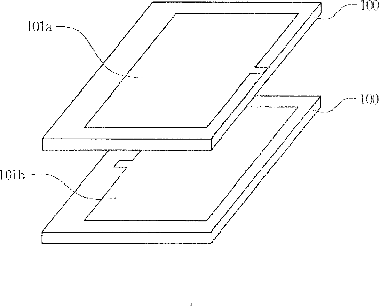
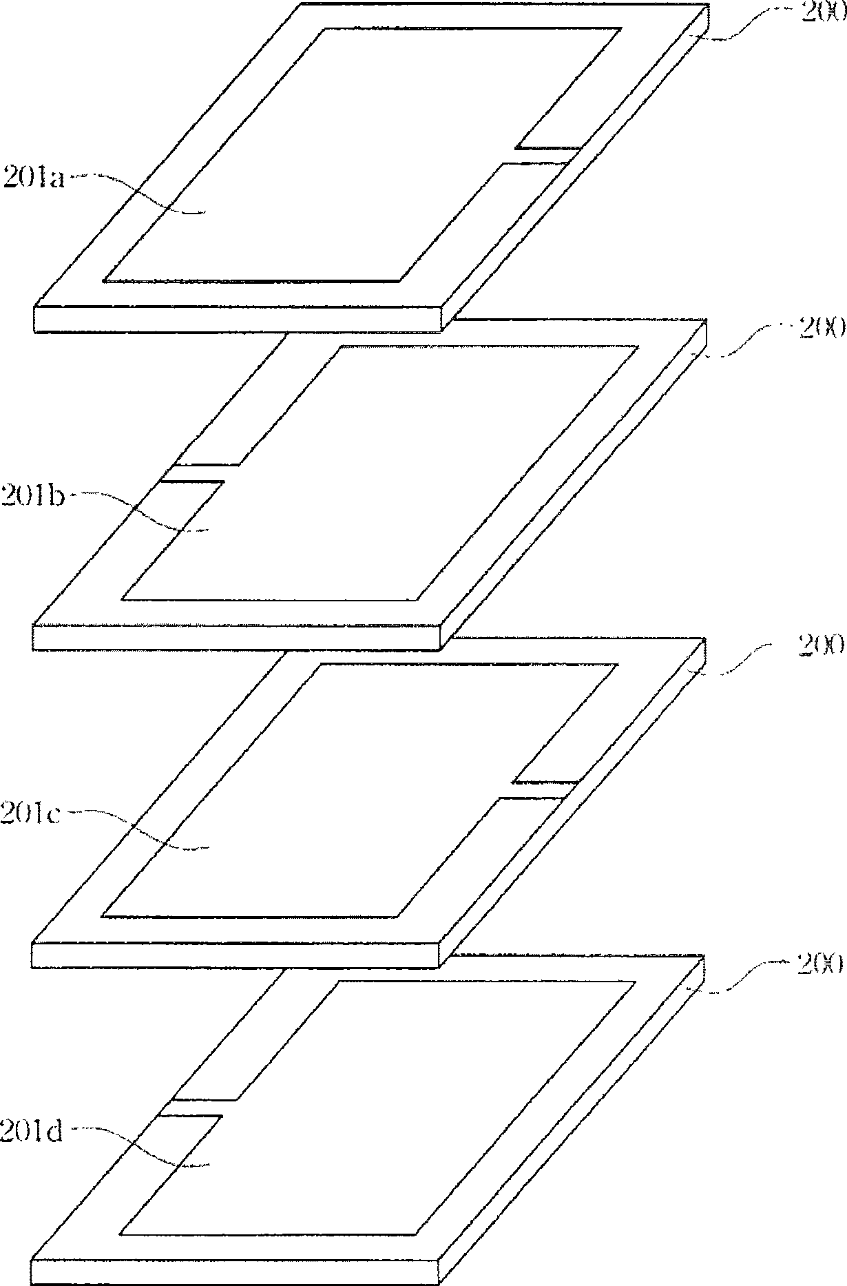
[0018] An embodiment of the present invention is to provide a die-carrying packaging substrate with embedded passive elements. In order to make the above and other purposes, features, and advantages of the present invention more comprehensible, a die-carrying packaging substrate 300 embedded with an embedded capacitor 30 is taken as a preferred embodiment for illustration.

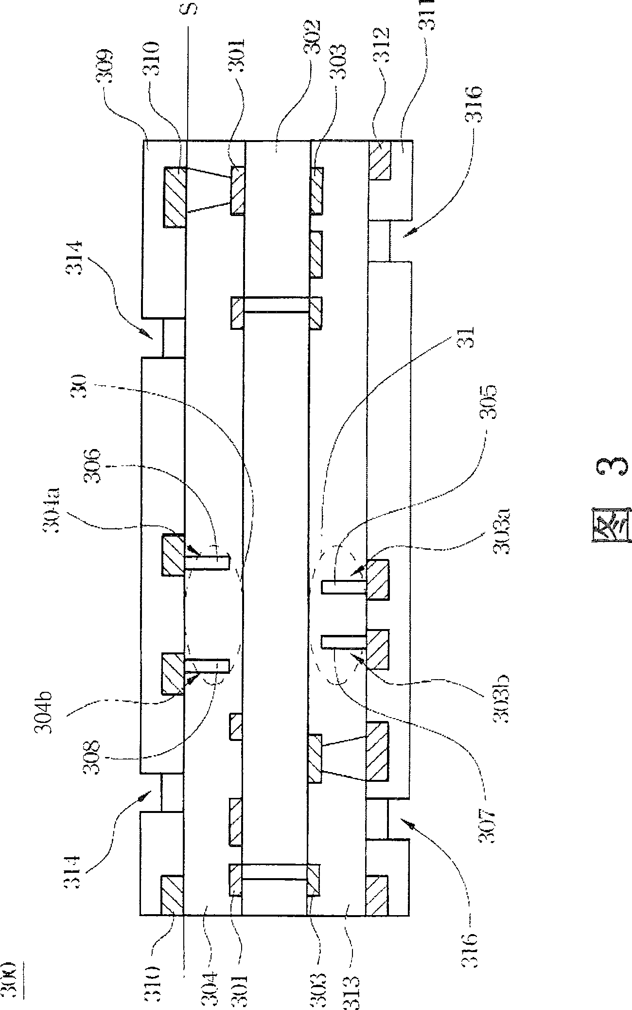
[0019] FIG. 3 is a cross-sectional view of a longitudinal structure of a die-carrying packaging substrate 300 embedded with an embedded capacitive element 30 according to a preferred embodiment of the present invention. The package substrate 300 for carrying dies includes: a lower lamination layer 313 , an interlayer circuit board 302 with a first conductive circuit 301 , a dielectric layer 304 , a first electrode 306 , a second electrode 308 and a second ...


PUM


Abstract

The disclosed base plate includes interlaid circuit board of possessing first conducting circuit, dielectric layer, first electrode, second electrode, and second conducting circuit. Being setup on the interlaid circuit board, the dielectric layer possesses first concave hole and second concave hole. First electrode is setup in the first concave hole, and the second electrode is setup in the second concave hole. The first and second electrodes as well as the dielectric layer located between first electrode and second electrode constitute an embedded passive element jointly. Second conducting circuit connects first electrode and second electrode electrically.

Description

technical field [0001] The invention relates to a packaging structure and a manufacturing method thereof, in particular to a packaging substrate for carrying a die with embedded passive elements and a manufacturing method thereof. Background technique [0002] The embedded capacitor element structure is a structure in which the capacitor is embedded in the substrate with a dielectric material by using a multi-layer circuit board package (Multiple Stacked Package; MSP) technology according to the circuit characteristics and requirements of the module. In actual application, substrate materials with different dielectric numbers and resistances can be used in the design of embedded capacitors, resistors, or high-frequency transmission lines according to circuit characteristics and requirements. Through the assembly and integration of embedded component substrate technology, the circuit layout and signal transmission distance are shortened to improve the performance of the overa...

Claims


Application Information

Patent Timeline
Patent Type & Authority Patents(China)
IPC IPC(8): H01L21/48H01L21/60H01L23/488H05K3/32H05K1/18
CPCH01L2924/0002
Inventor 王永辉欧英德洪志斌
Owner ADVANCED SEMICON ENG INC
Why Eureka
Try Eureka