Page-buffer and non-volatile semiconductor memory including page buffer
A non-volatile, memory technology, used in static memory, read-only memory, memory systems, etc., to solve problems such as occupying space resources
- Summary
- Abstract
- Description
- Claims
- Application Information
AI Technical Summary
Problems solved by technology
Method used
Image

Examples
Embodiment Construction
[0058] In the following, the invention will be illustrated by means of preferred but non-limiting examples.
[0059] Figure 11 A block diagram of a nonvolatile semiconductor memory device according to an embodiment of the present invention is shown.
[0060] refer to Figure 11 , the nonvolatile semiconductor memory device of this example includes a memory cell array MCARR, a page buffer block NWPBB, first and second global input lines GDI and nGDI, a global output line GDOUT, a y address signal line Yp , Yq and Yr, read latch signal line LCH, and page buffer decoder NWDE.
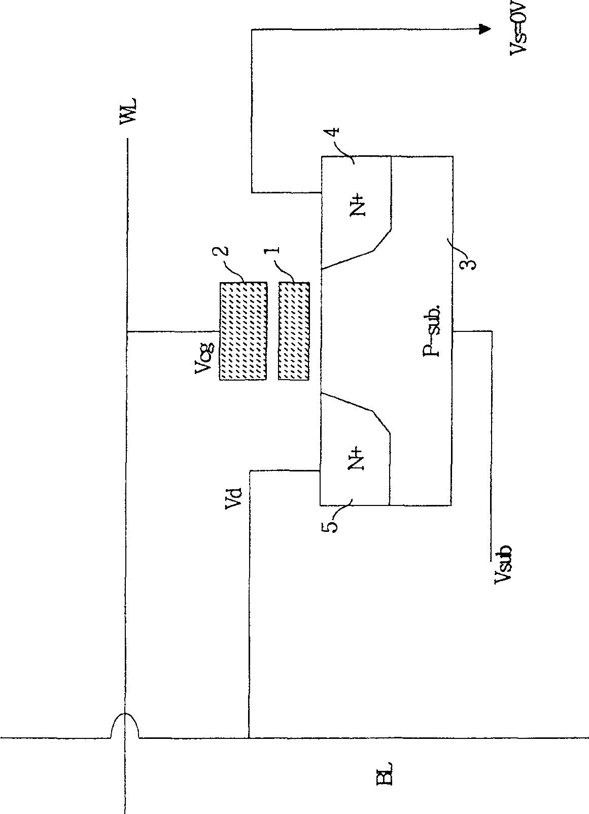
[0061] The memory cell array MCARR includes a matrix array of memory cells, word lines WL (not in Figure 11 shown in ) and bit lines BL. In the example of this embodiment, the memory cells are flash memory cell transistors.
[0062] Connect the internal input lines IDI and nIDI, and the internal output line IDOUT between the page buffer decoder NWDE and the corresponding page buffer blo...
PUM
 Abstract
Description
Claims
Application Information
 - R&D Engineer
- R&D Manager
- IP Professional
- Industry Leading Data Capabilities
- Powerful AI technology
- Patent DNA Extraction
Browse by: Latest US Patents, China's latest patents, Technical Efficacy Thesaurus, Application Domain, Technology Topic.
© 2024 PatSnap. All rights reserved.Legal|Privacy policy|Modern Slavery Act Transparency Statement|Sitemap